Blog
This blog post details APD's comprehensive die sort, pick, place, and labeling services, emphasizing their critical role in the semiconductor manufacturing process. It covers the benefits of each service and explains how APD’s advanced technologies ensure precise, efficient, and reliable outcomes for various applications.
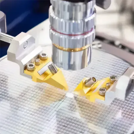
This blog post highlights APD's capabilities in dicing 300mm wafers, emphasizing the economic advantages of larger wafers in semiconductor manufacturing. It covers the services APD provides, including mounting, dicing, inspection, and more, and explains why APD is a preferred choice for clients needing precise and efficient wafer dicing.
This blog focuses on APD's custom precision spacers and shims, designed to meet specific client requirements. It discusses the benefits of using APD’s turnkey services, which include custom sizing, coatings, and laser markings, and how they streamline the production process, saving time and money.
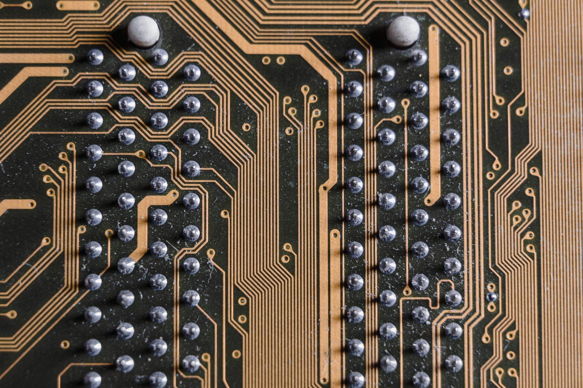
This post offers a thorough overview of various PCB depaneling methods, including laser depaneling, die-punching, hand depaneling, and wafer dicing saws. It discusses the advantages and applications of each method, helping readers understand how to choose the right approach for their specific PCB manufacturing needs.
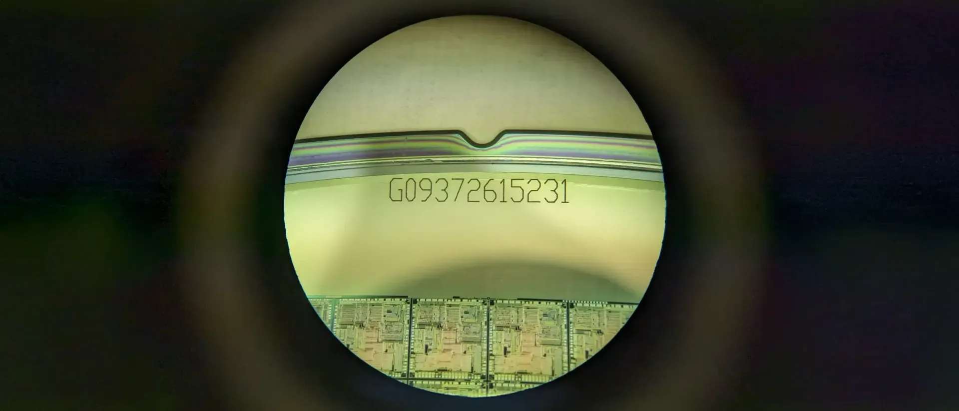
This blog outlines the laser marking services offered by APD, detailing their applications across various industries. It explains how APD's advanced laser technology provides precise, durable, and customizable markings on a wide range of materials, including metals, ceramics, and semiconductors. The post emphasizes the benefits of laser marking, such as high resistance to wear and corrosion, making it an ideal solution for product identification and traceability.
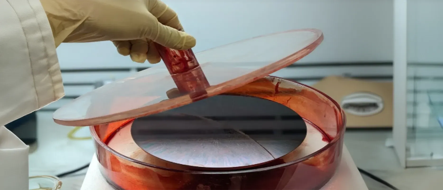
This blog post explores APD’s expertise in photoresist application, a crucial step in wafer processing for semiconductor manufacturing. It explains the importance of photoresist in protecting wafer surfaces during etching and other processes, highlighting APD's commitment to precision and quality in every step. The post also covers the types of materials handled and the advanced techniques used to ensure optimal results.
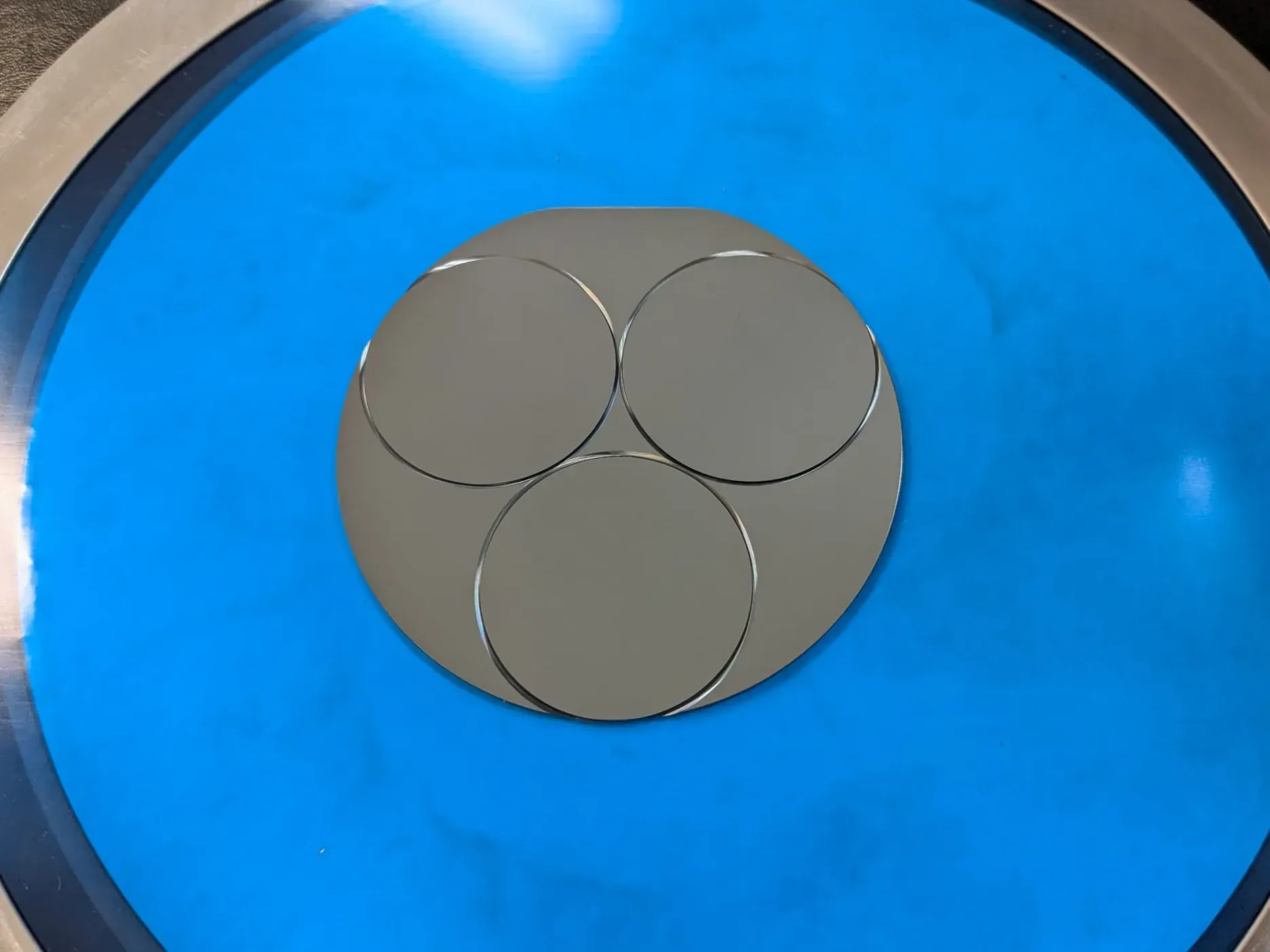
Discover APD’s specialized wafer coring services, where precision meets versatility. This blog post delves into the wafer coring process, highlighting how APD uses state-of-the-art equipment to core wafers of various materials, including silicon, glass, and ceramics. Learn about the benefits of our custom coring solutions, designed to meet the specific needs of semiconductor and microelectronics industries.
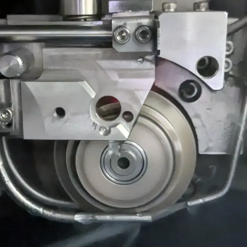
This blog explores the intricate process of wafer dicing at American Precision Dicing, Inc. (APD). It delves into the meticulous steps involved, from material preparation to quality assurance, highlighting APD's expertise in handling various hard and brittle materials. The post also emphasizes APD's commitment to speed, value, and flexibility, making them a trusted partner in semiconductor manufacturing.
