Laser Marking: Enhancing Component Identification in Semiconductor Manufacturing
High-precision laser marking for reliable component identification
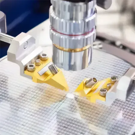
In the semiconductor industry, the need for precise, durable, and easily traceable components is paramount. Laser marking is a vital process that meets these demands, providing clear, permanent markings on semiconductor wafers and components. At American Precision Dicing (APD), we excel in delivering high-quality laser marking services tailored to the specific needs of our clients.
What is Laser Marking?
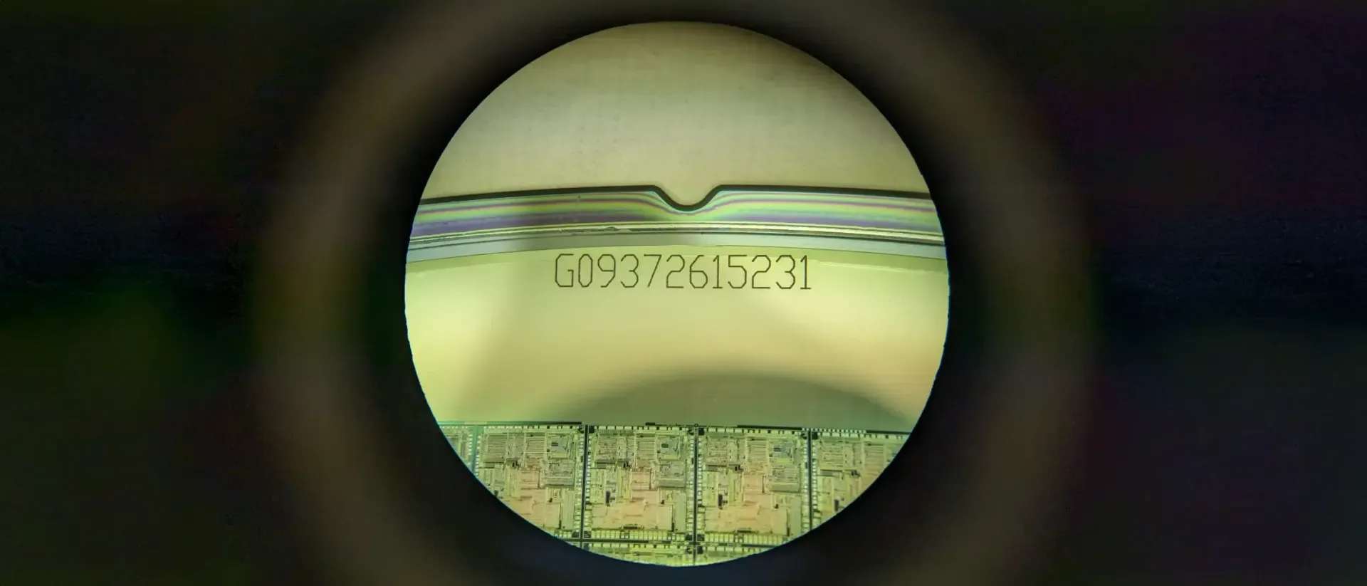
Laser marking involves the use of a focused laser beam to etch or engrave detailed information onto semiconductor materials. These markings can include serial numbers, barcodes, logos, or other critical identification data. The process is non-contact, ensuring that the wafers and components remain undamaged and maintain their integrity throughout the manufacturing process.
The Laser Marking Process
1.
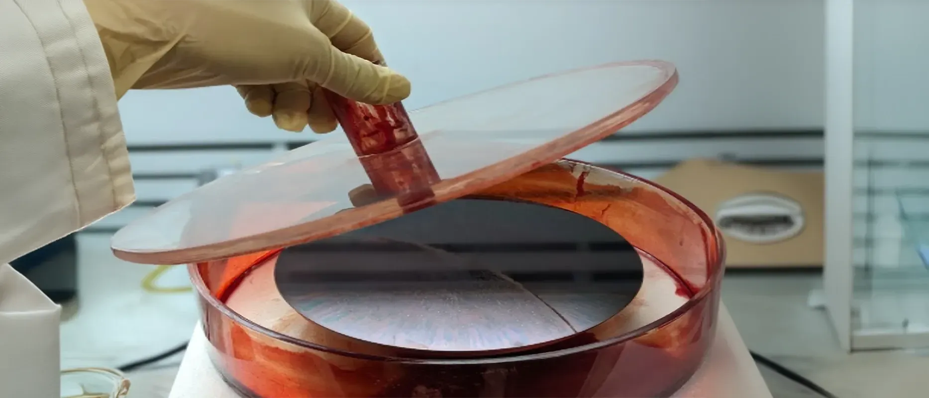
Material Preparation:
The surface of the wafer or component is cleaned and prepared for marking.
2.
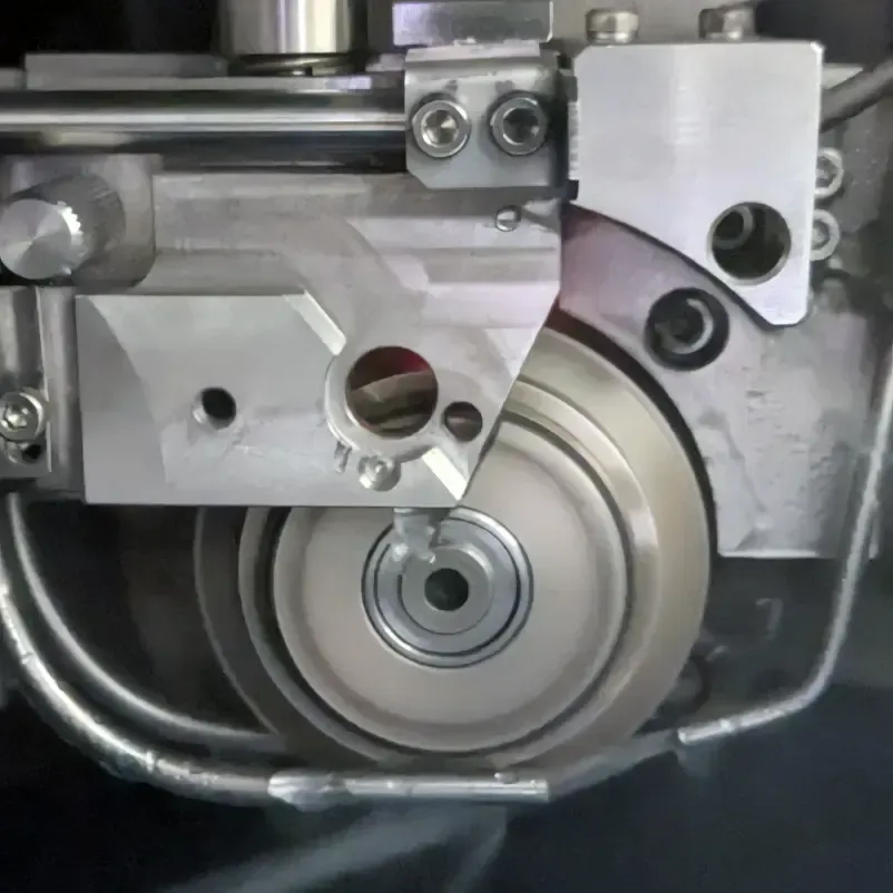
Precision Marking: A laser engraves the required information onto the material. The laser’s intensity and speed are carefully controlled to achieve the desired mark without damaging the material.
3.
Verification:
Each marked wafer is inspected for clarity and accuracy to ensure compliance with industry standards.
4.
Packaging: After marking and inspection, wafers are carefully packaged to prevent any damage during transportation.
Applications of Laser Marking
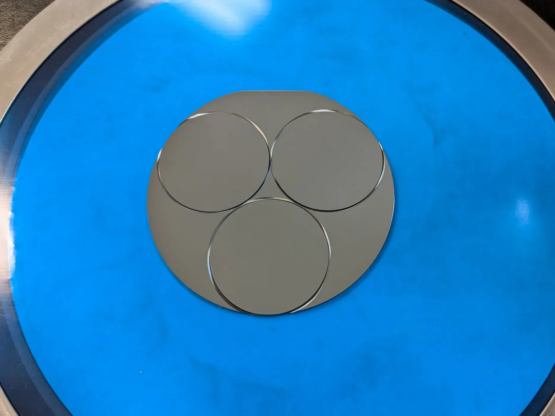
Laser marking is used across various stages of semiconductor manufacturing, including wafer identification, component tracking, and branding. Its versatility makes it suitable for a wide range of materials, such as silicon, ceramics, and metals, ensuring that every component can be reliably identified throughout its lifecycle.
Why Choose APD for Laser Marking?
1.
Unmatched Precision: Our state-of-the-art laser marking systems ensure that each mark is made with the highest accuracy, even on the smallest components.
2.
Durability: Laser markings are permanent and resistant to wear, ensuring that the information remains legible throughout the component’s use.
3. Customization: We offer tailored marking solutions to meet the specific needs of your project, from serial numbers to complex logos.
Conclusion
Laser marking is an essential service in semiconductor manufacturing, providing the traceability and precision required in today’s high-tech industry. At APD, we are committed to delivering top-tier laser marking services that meet the exacting standards of our clients. Contact us today to learn how our laser marking services can enhance your manufacturing process.
For more information, visit our
Laser Marking Service Page.