Precision Wafer Dicing Services
Tailored to Your Needs
American Precision Dicing (APD)
is a
fast turn wafer dicing service
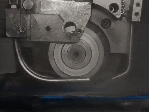
that has been providing a variety of services since 1999. We use precision mechanical dicing saws with diamond dicing blades to dice, cut, core, downsize and machine a large variety of wafers made of various types and combinations of hard brittle materials. We have diced, cut, cored and scribed wafers of silicon, glass, ceramics, sapphire, silicon carbide and many other materials.
We service Universities, R&D departments of large companies, low to medium volume production operations, start-ups and Research Labs (both Private and Federal). We do small to medium size jobs on a fast turn basis.
With cutting-edge equipment and years of expertise, APD can deliver wafer dicing solutions tailored to exacting standards.
Our process capabilities include:
- Make cuts as thin as 20 microns wide
- Perform trenching with variations in depths to < 5 micrometers over a 300-millimeter cut.
- Process wafers as thin as 50 microns
- Cut wafers as thick as 10 mm
- Cut a wide range of wafer sizes up to 300 mm in diameter
Comprehensive Overview of Wafer Dicing Techniques and Processes
Wafer dicing (also known as wafer scribing, wafer cutting or die singulation) is the precise process of separating individual semiconductor dies from a larger wafer, a critical final step in semiconductor manufacturing. As the demand for intricate microelectronic components grows, wafer dicing has evolved to include various specialized techniques to meet diverse requirements for material type, precision, and project scale.
Since the 1950s, wafer dicing has evolved significantly, with multiple methods now available for precise singulation of semiconductor materials. Below, we outline the primary methods used today, including both in-house processes at APD and those managed through trusted partners. Some of these techniques are included for reference only to provide a comprehensive background on wafer dicing.
1. Mechanical Singulation Processes
Mechanical sawing methods include Scribe and Break, Wafer Sawing with a diamond blade, and Dicing Before Grinding (DBG). Scribe and Break is a dry process ideal for singulating microelectromechanical (MEMS) devices and other sensitive materials, though it can become challenging with thicker substrates. Wafer Sawing, the most commonly requested process, uses diamond blades to achieve clean, precise cuts, particularly for silicon wafers.
2. Laser Singulation Processes
Laser dicing methods include laser ablation, stealth laser dicing, and thermal laser separation. Stealth laser dicing, a process that creates internal modifications in the wafer, is particularly effective for MEMS devices and provides a clean, efficient singulation. Laser ablation, another precise method, is often chosen when standard mechanical cuts aren't suitable.
3. Alternative Singulation Processes
Plasma dicing is an emerging technology offering speed and cost advantages for large wafers with very small die sizes. Although APD primarily focuses on mechanical and laser processes, plasma dicing and other advanced techniques continue to expand the capabilities of the industry.
THE APD PROCESS
A Step-by-Step Guide to APD’s Precision Wafer Dicing Process
At American Precision Dicing, we are committed to delivering precise, reliable wafer dicing services through a structured, end-to-end process designed for accuracy and customer satisfaction. Each project is carefully managed from the initial discussion to the final shipment, ensuring every detail aligns with the client's specifications and industry standards. Our process typically follows these stages:
1. Project Communication
We begin by discussing project specifications with the customer via email or phone to fully understand their requirements.
2. Quotation and Order Acceptance
A detailed quote is prepared and sent for approval. Once accepted, the customer ships the materials to our facility.
3. Material Receipt and Inspection
Upon arrival, all materials are inspected to ensure they are intact. Any issues are promptly communicated to the customer.
4. Production Planning
The production manager creates a tailored processing plan, referencing both industry expertise and our extensive database of prior projects.
5. Surface Protection (if needed)
If the wafer surface requires protection, we apply a protective layer to safeguard it during processing.
6. Mounting and Blade Preparation
The material is mounted and allowed to cure, and the appropriate diamond blade is selected, installed, and dressed for the task.
7. Dicing and Washing
The wafer is diced/cut according to the customer’s exact specifications, followed by a high-pressure wash to ensure a clean, dust-free surface.
8. Quality Assurance
The diced wafer undergoes a thorough inspection in QA, with a detailed report provided.
9. Packaging and Shipping
Once cleared by QA, the wafer is securely packaged and shipped to the customer.
10. Invoicing
Following shipment, an invoice is sent to the customer, completing the order.
APD’s comprehensive wafer dicing process ensures the highest standards of accuracy, quality, and quick turnaround, supported by our decades of experience and expertise in semiconductor services. Our precision-driven approach minimizes chipping and ensures clean, consistent cuts, making us a trusted partner for industries requiring exceptional reliability.
Partner with APD for Your Wafer Dicing Needs
At American Precision Dicing (APD), we specialize in providing high-precision wafer dicing solutions to meet the unique requirements of your projects. Our experienced team is dedicated to delivering exceptional quality and fast turnaround times, ensuring your project's success.
Our Wafer Dicing Services Include:
- Custom dicing for various wafer materials
- Advanced techniques to minimize chipping and damage
- Flexible solutions for both small and large-scale productions
Ready to Discuss Your Project? Contact us today to learn more about how our wafer dicing services can benefit your application.
📩 Request a Quote | 📞 Contact Us
Let APD be your trusted partner in achieving precision and excellence in wafer dicing.
