The Crucial Role of Photoresist in Semiconductor Manufacturing
Enhancing semiconductor fabrication with expert photoresist handling.
In the advanced world of semiconductor manufacturing, photoresist materials play a vital role in achieving the high precision required for modern devices. At American Precision Dicing, Inc. (APD), we leverage our expertise in photoresist application to ensure optimal results in our wafer dicing services. This blog post explores the importance of photoresist and its application in our processes.
Understanding Photoresist
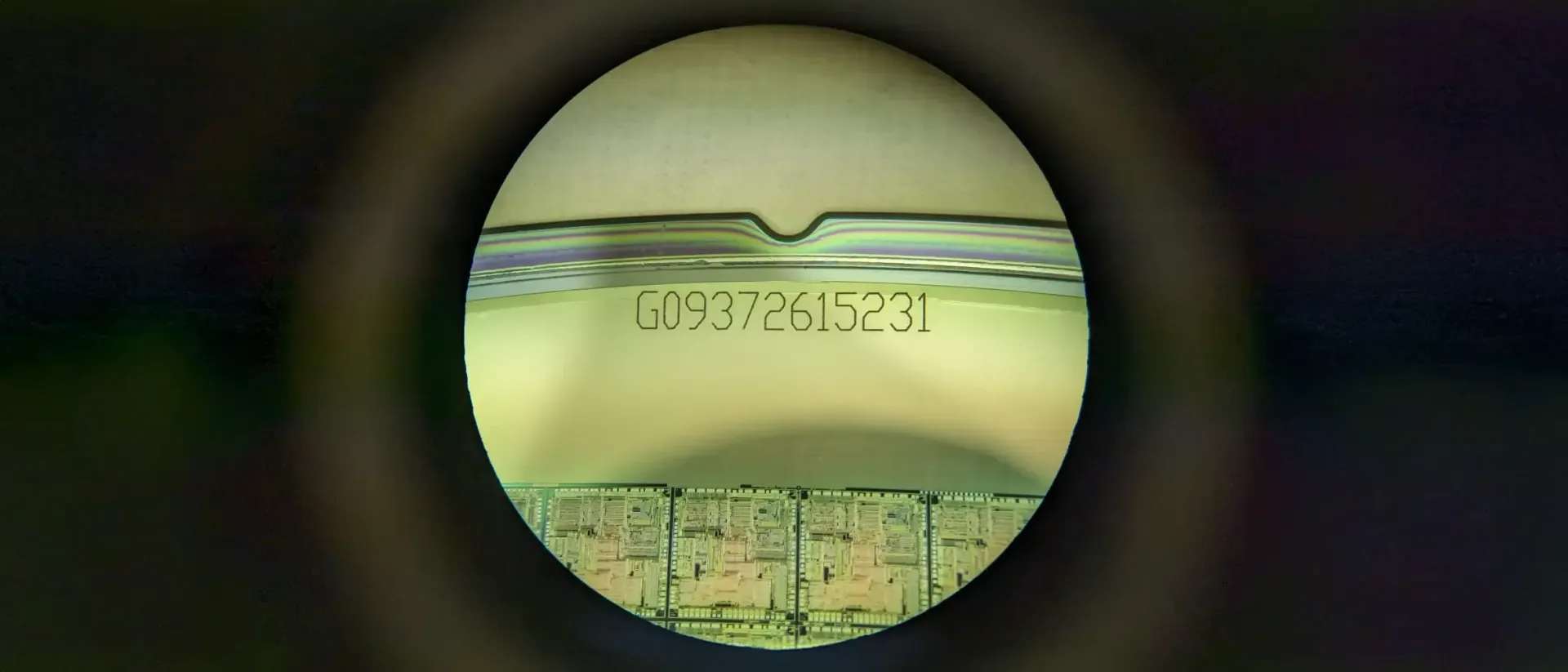
Photoresist is a light-sensitive material used to form a patterned coating on a surface. In semiconductor manufacturing, it is essential for defining intricate circuit patterns on wafers. There are two main types of photoresist: positive and negative. Positive photoresist becomes soluble when exposed to light, allowing the exposed areas to be removed, while negative photoresist becomes insoluble, leaving the exposed areas intact.
The Dicing Process and Photoresist
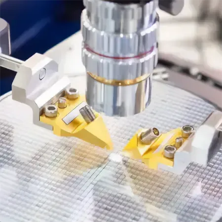
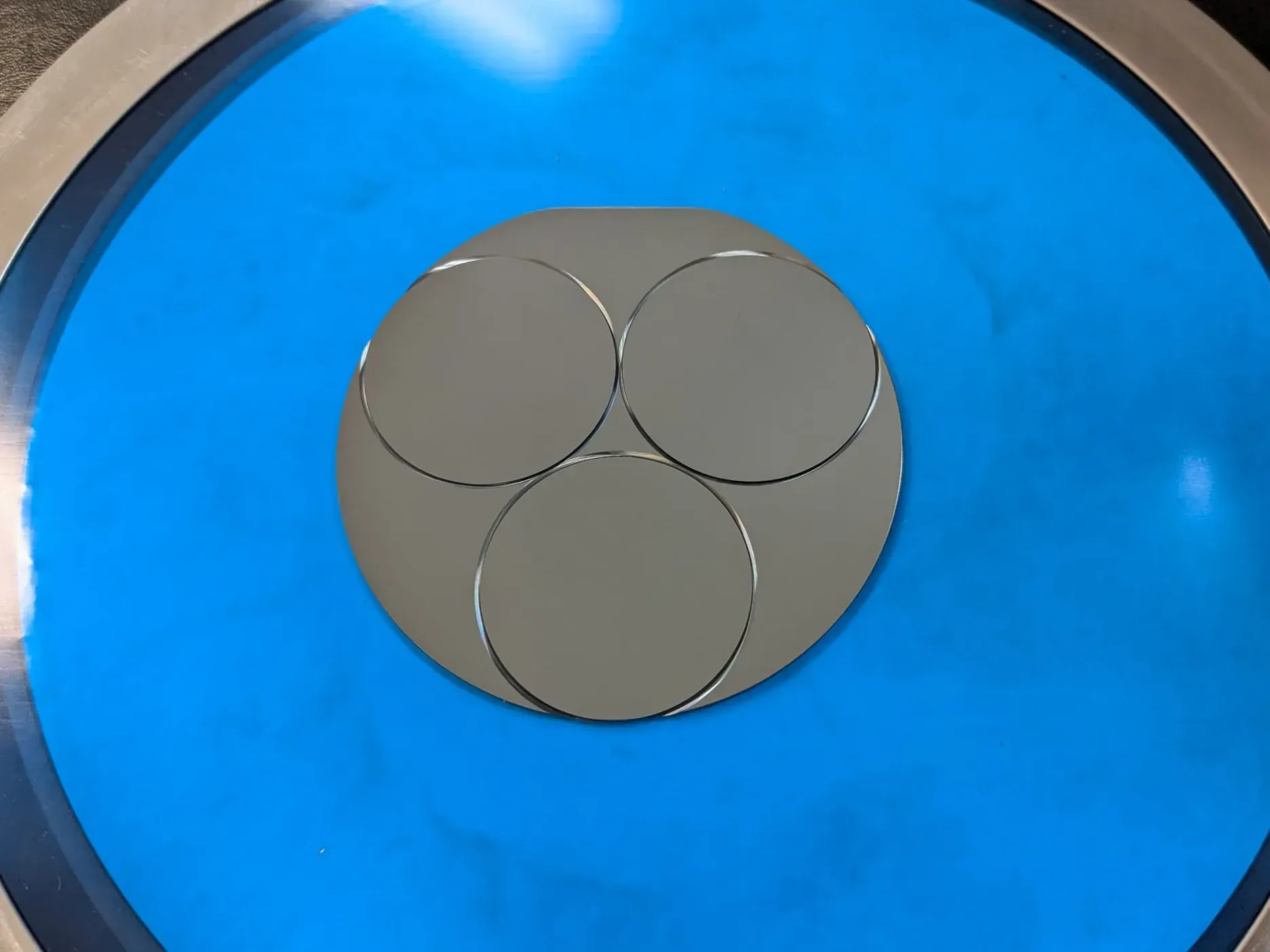
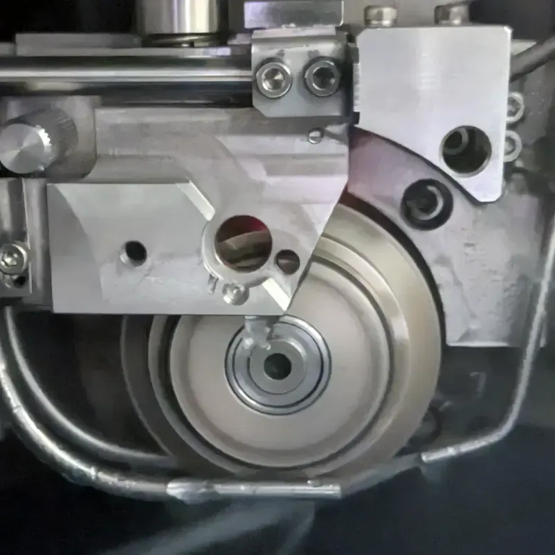
The dicing process, also known as wafer sawing, involves segmenting a large silicon wafer into individual dies or integrated circuits (ICs) using a thin abrasive blade. This rotating blade can launch particles at high speeds, necessitating extra protection for the wafer’s surface. Traditionally, photoresist has been used to protect the wafer during this critical step.
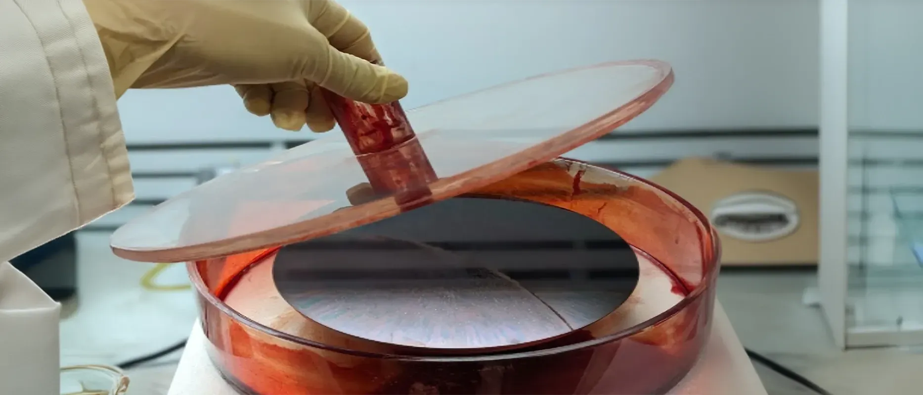
1. Photoresist Application: The photoresist is applied to the wafer surface via spin coating. When exposed to specific wavelengths of light, the photoresist hardens in the exposed areas, allowing selective removal of the soluble unexposed areas using a developer solution.
2. Surface Protection:
In the context of dicing, the photoresist acts as a sacrificial layer, absorbing the initial impact of the dicing blade and minimizing chipping or damage to the underlying silicon die.
3. Removal Process:
After dicing is complete, the remaining photoresist is removed using a cleaning process that typically involves acetone, alcohol, and DI water.
The Role of Water in Dicing
Modern dicing saws utilize flooding bars to cool the blade, provide lubrication, and remove debris from the cutting kerf, creating a thin water layer on the wafer’s surface. This water layer acts similarly to photoresist by absorbing the initial impact of particles, thus mitigating damage to the die surface.
When is Photoresist Recommended?
While the water layer offers sufficient protection in many dicing applications, using photoresist can be beneficial in specific situations:
- Protection of Sensitive Structures: Wafers with delicate features benefit from the added protection of photoresist.
- Debris Reduction: Photoresist acts as a barrier to prevent silicon dust and debris from contaminating the wafer's surface and makes debris easier to remove afterward.
- Chipping Prevention: A photoresist layer helps minimize the risk of chipping along the edges of dies.
Advanced Capabilities and Custom Solutions
At APD, we pride ourselves on our ability to handle both standard and custom photoresist applications. Our advanced equipment and expertise allow us to offer tailored solutions that meet the specific needs of our clients, ensuring the highest quality results.
Why Choose APD?
Choosing APD means partnering with a company that prioritizes precision, reliability, and customer service. Our decades of experience and commitment to excellence ensure that we deliver top-tier photoresist application services that enhance your semiconductor manufacturing processes.
Conclusion
Photoresist is a cornerstone of semiconductor manufacturing, and at APD, we excel in providing this essential service with unmatched precision and reliability. Our comprehensive process, advanced capabilities, and dedication to customer satisfaction make us the ideal partner for your photoresist needs. Explore our services and see how we can enhance your manufacturing process with our expertise and dedication.
For more information on our photoresist services, please visit
APD's Photoresist Service Page.