Blog Layout

Custom Precision Spacers and Shims

Optimize Your Prototyping and Testing with Custom Precision Parts

Custom Precision Spacers and Shims

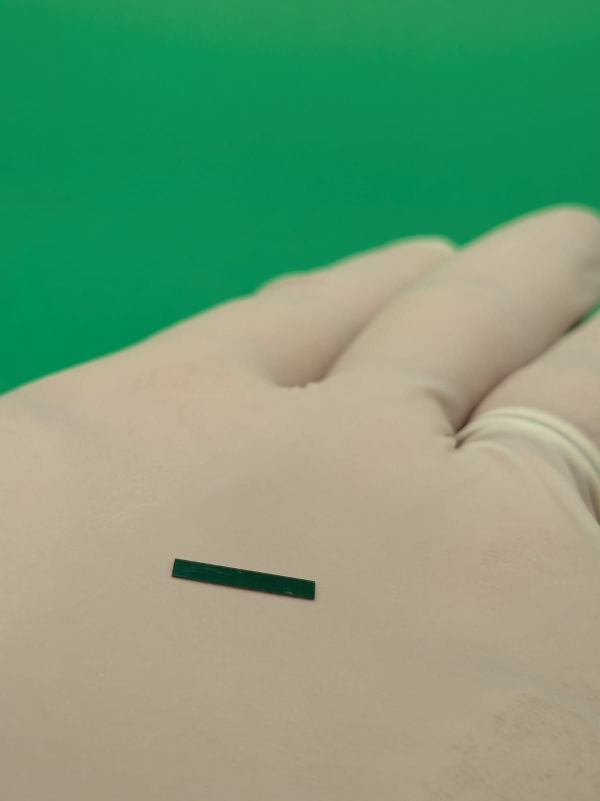
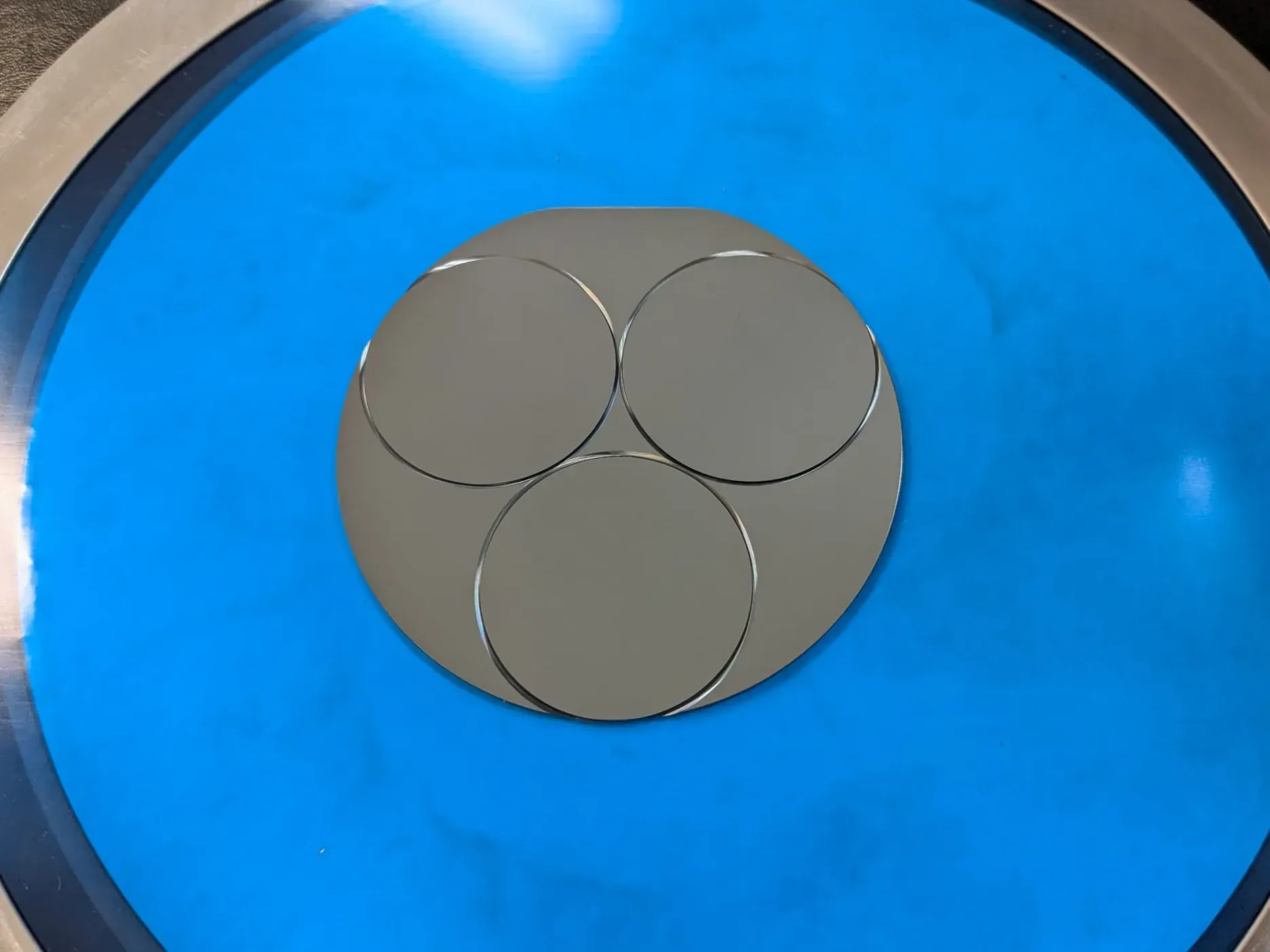
APD offers turnkey custom chips designed to serve as shims, spacers, and coupons for various applications, including prototyping and testing. Our ready-to-use parts can be laser marked with serial numbers, part numbers, or bar codes, providing a complete solution that saves you time, money, and hassle.

What We Provide


At APD, we specialize in creating custom precision spacers and shims tailored to your specific requirements. Our offerings include:

Materials: We work with non-metallic materials such as silicon, glass, and sapphire.
Dimensions: Precisely crafted to your X, Y, and Z measurements.
Optional Customizations: Choose from custom coatings or specialized laser markings for easy identification.

These components are ideal for a range of industries, including semiconductor manufacturing, aerospace, and medical devices, where precision and reliability are paramount.

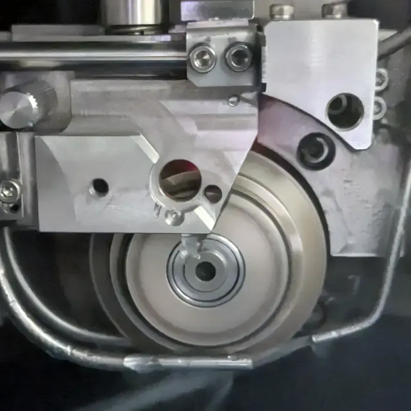
The Traditional DIY Approach

Typically, creating custom shims and spacers involves a complex, multi-step process:

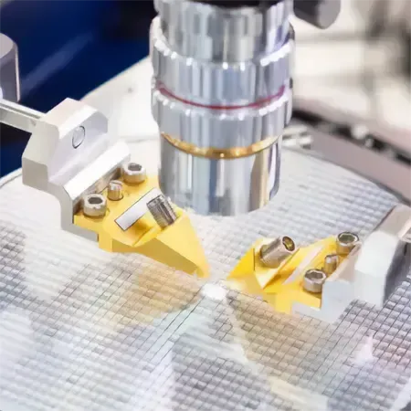
  1. Source a wafer from a wafer house.
  2. Backgrind the wafer to the desired thickness.
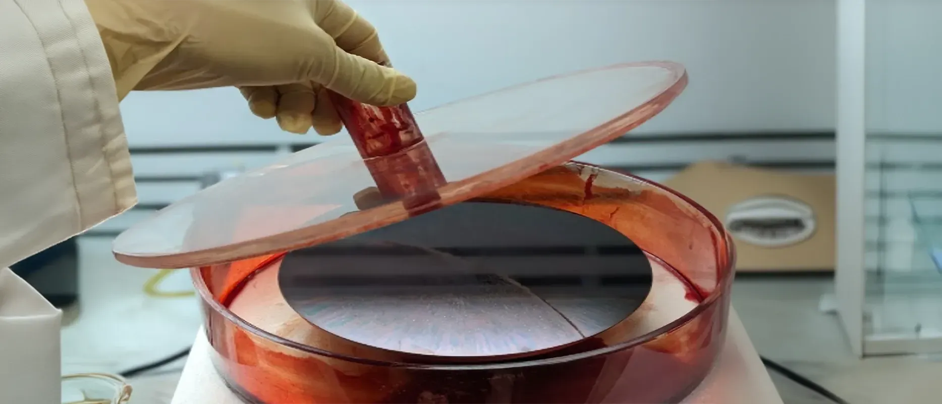
  3. Polish the wafer if required.
  4. Apply the oxide layer or other coatings.
  5. Arrange for dicing services to cut the wafer.
  6. Add serial numbers or other identifiers.
  7. Package the parts in waffle packs, gel-paks, or on tape and ring.

This approach not only consumes valuable time but also increases the risk of errors at each stage.

The APD Advantage

Why go through the hassle of coordinating multiple vendors when APD can handle the entire process for you? Our end-to-end service ensures that you receive high-quality, custom-made spacers and shims that meet your exact specifications, delivered quickly and efficiently.

If you're interested in our custom precision spacers and shims service, contact us at +1(408)539-9880, sales@wafer-dicing.com, or visit our Request a Quote page to get started. Let us help you achieve precision and efficiency in your semiconductor manufacturing processes.

Die Sort, Pick, Place, and Labeling Inspection
August 26, 2024
This blog post details APD's comprehensive die sort, pick, place, and labeling services, emphasizing their critical role in the semiconductor manufacturing process. It covers the benefits of each service and explains how APD’s advanced technologies ensure precise, efficient, and reliable outcomes for various applications.
Wafer Dicing Machine
August 26, 2024
This blog post highlights APD's capabilities in dicing 300mm wafers, emphasizing the economic advantages of larger wafers in semiconductor manufacturing. It covers the services APD provides, including mounting, dicing, inspection, and more, and explains why APD is a preferred choice for clients needing precise and efficient wafer dicing.
PCB - Printed Circuit Board
August 26, 2024
This post offers a thorough overview of various PCB depaneling methods, including laser depaneling, die-punching, hand depaneling, and wafer dicing saws. It discusses the advantages and applications of each method, helping readers understand how to choose the right approach for their specific PCB manufacturing needs.
Laser Marking Banner
August 19, 2024
This blog outlines the laser marking services offered by APD, detailing their applications across various industries. It explains how APD's advanced laser technology provides precise, durable, and customizable markings on a wide range of materials, including metals, ceramics, and semiconductors. The post emphasizes the benefits of laser marking, such as high resistance to wear and corrosion, making it an ideal solution for product identification and traceability.
Photoresist Application
August 12, 2024
This blog post explores APD’s expertise in photoresist application, a crucial step in wafer processing for semiconductor manufacturing. It explains the importance of photoresist in protecting wafer surfaces during etching and other processes, highlighting APD's commitment to precision and quality in every step. The post also covers the types of materials handled and the advanced techniques used to ensure optimal results.
Wafer Coring
August 12, 2024
Discover APD’s specialized wafer coring services, where precision meets versatility. This blog post delves into the wafer coring process, highlighting how APD uses state-of-the-art equipment to core wafers of various materials, including silicon, glass, and ceramics. Learn about the benefits of our custom coring solutions, designed to meet the specific needs of semiconductor and microelectronics industries.
Wafer Dicing Machine cutting a wafer
July 3, 2024
This blog explores the intricate process of wafer dicing at American Precision Dicing, Inc. (APD). It delves into the meticulous steps involved, from material preparation to quality assurance, highlighting APD's expertise in handling various hard and brittle materials. The post also emphasizes APD's commitment to speed, value, and flexibility, making them a trusted partner in semiconductor manufacturing.
Share by: