Die Sort, Pick, Place, and Labeling: Precision Handling for Semiconductor Dies
Ensuring Accuracy, Efficiency, and Traceability in Semiconductor Manufacturing

In semiconductor manufacturing, precision is paramount. The processes of die sorting, picking, placing, and labeling are critical in ensuring that each semiconductor die meets the highest standards of quality. At American Precision Dicing, Inc. (APD), we leverage advanced technology and expertise to offer die handling services that enhance productivity, reduce waste, and ensure accuracy throughout the manufacturing process.
Understanding Die Sort, Pick, Place, and Labeling
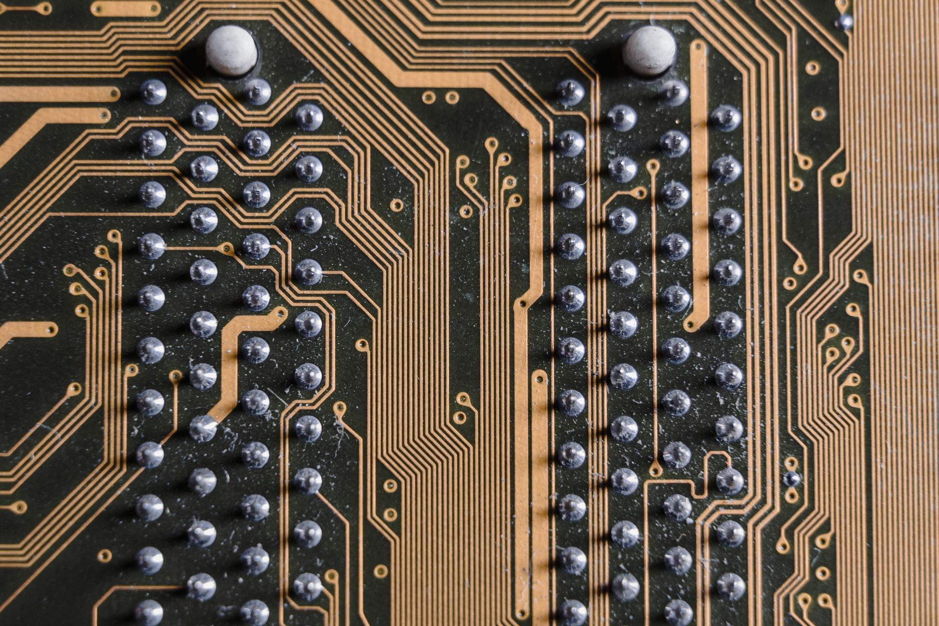
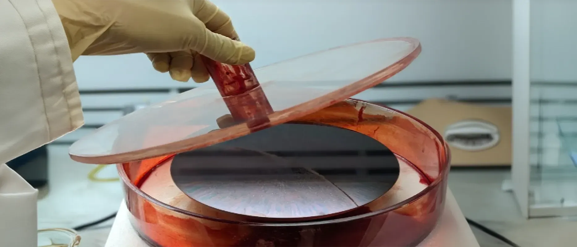
Die Sorting: After wafer dicing, the dies are inspected to separate functional dies from defective ones. This step is crucial as it determines the quality of the final product. At APD, our sorting systems use optical and electrical testing to ensure only the best dies proceed to the next stage.
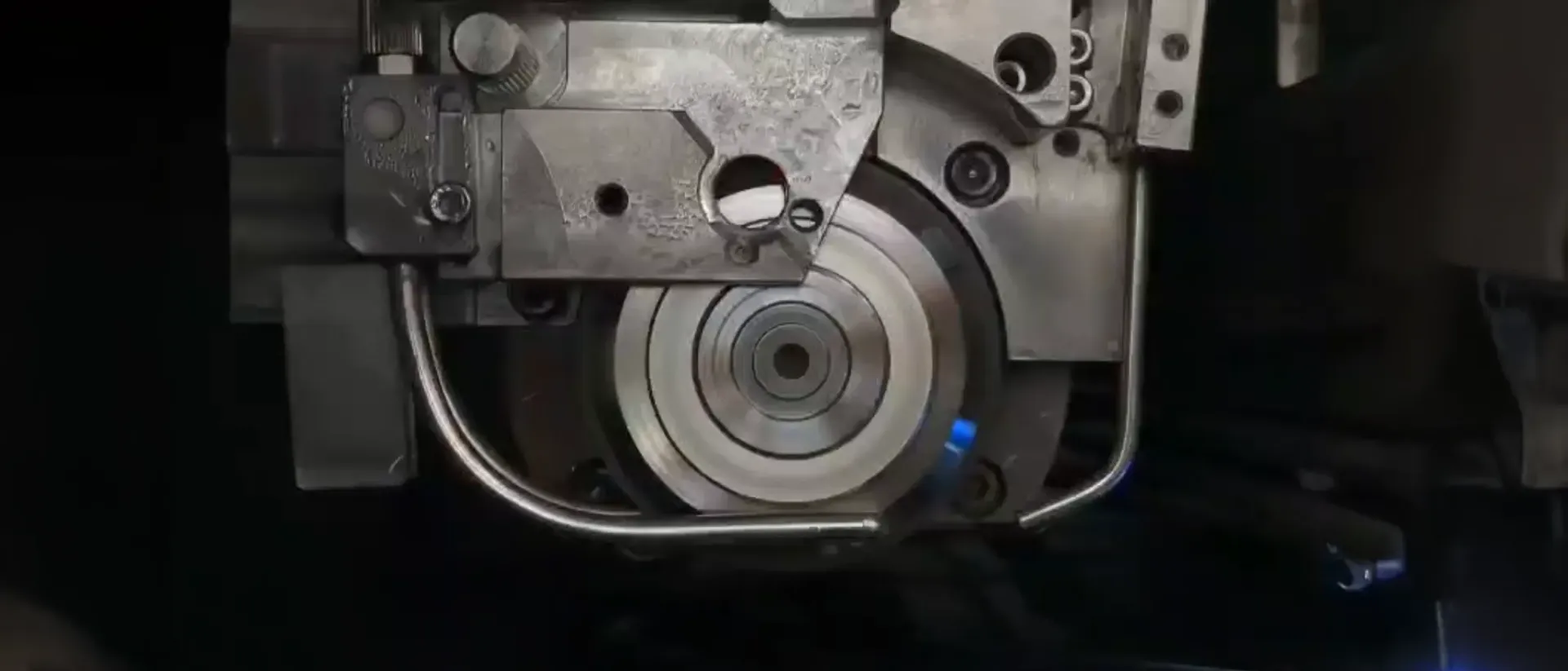
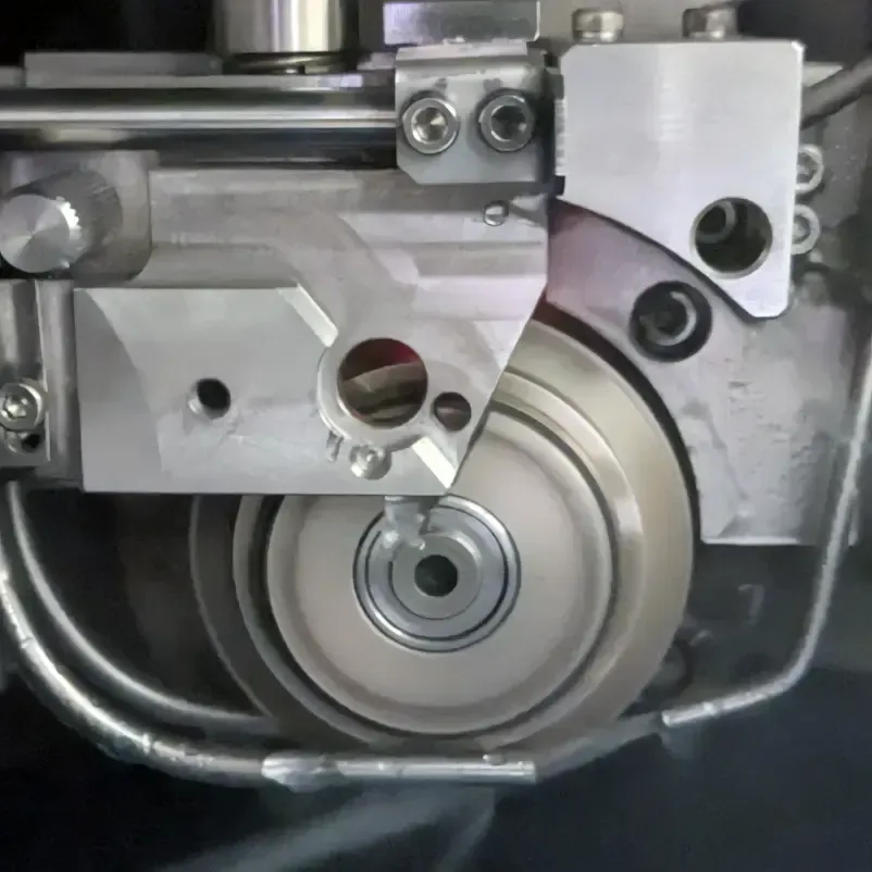
Die Picking: Once sorted, functional dies are carefully picked from the wafer. APD’s automated pick-and-place machines handle this with precision, minimizing the risk of damage and ensuring that dies are ready for packaging or further processing.
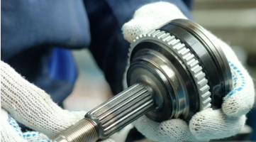
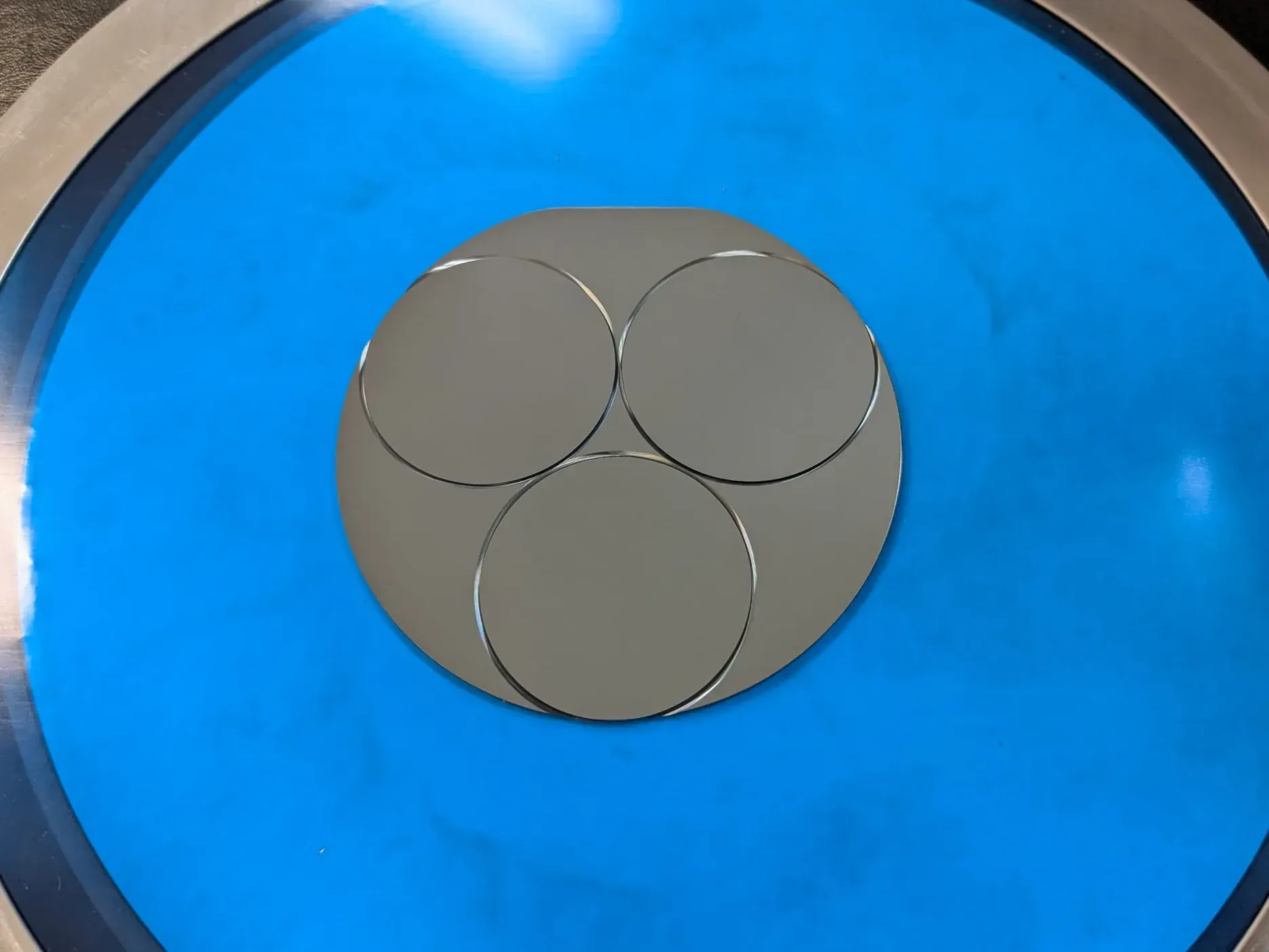
Die Placing: After picking, dies need to be accurately placed onto carriers, substrates, or lead frames. Precision in placement is essential for the subsequent bonding and packaging processes. APD’s high-precision equipment ensures that each die is placed with exact alignment, supporting both low and high-volume production.
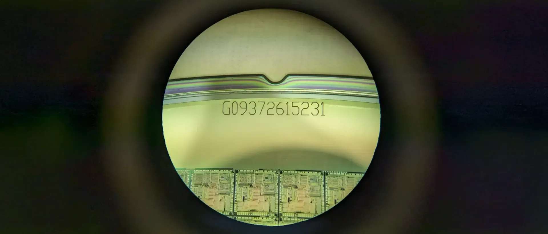
Labeling: Accurate labeling is essential for traceability, quality control, and compliance with industry standards. At APD, we offer advanced labeling solutions, including laser marking, which provides durable and precise identification of each die. This ensures that every die can be tracked throughout the manufacturing and distribution process.
Why Choose APD for Die Handling?
1.
Advanced Technology: APD utilizes cutting-edge technology to deliver superior die sorting, picking, placing, and labeling services. Our equipment is designed to handle the delicate nature of semiconductor dies, ensuring accuracy and consistency.
2.
Experienced Team: With decades of experience in the semiconductor industry, APD’s team is well-versed in the complexities of die handling. Our expertise ensures that we can meet the unique needs of each client, providing customized solutions that enhance efficiency and product quality.
3.
Comprehensive Services: From initial sorting to final labeling, APD offers a full suite of die handling services. Our integrated approach ensures seamless transitions between each stage, reducing turnaround times and increasing overall productivity.
Conclusion
The processes of die sorting, picking, placing, and labeling are integral to the success of semiconductor manufacturing. At APD, we combine advanced technology with industry expertise to provide precise, reliable, and efficient die handling services. Whether you need high-volume production or specialized handling, APD is your trusted partner for all your semiconductor die processing needs.
For more details, visit our
Die Sort, Pick, Place, and Labeling Service Page.