A Guide to the Depanelization of Printed Circuit Boards
Depanelization of PCBs: A Guide to the Different Methods
Depanelization is the critical process of separating individual printed circuit boards (PCBs) from a larger panel after assembly and testing. This step is vital to ensuring the final product's quality and functionality. Given the diverse requirements of PCB projects, selecting the right depaneling method is essential to balance precision, efficiency, and cost.
These boards are typically made of a woven fiberglass cloth and a flame-resistant epoxy resin binder called FR-4, making precision in cutting vital to preserving the integrity of the boards. Here, we explore the various depaneling methods and their respective advantages.
Laser Depaneling
Laser depaneling is recognized as the most precise method for separating PCBs. It uses a focused laser beam to cut through the PCB material, typically FR-4, with unparalleled accuracy. The non-contact nature of the process minimizes the risk of mechanical stress or damage to the board, making it ideal for high-density or complex designs. Laser depaneling is particularly suited for high-volume production where consistent precision is paramount.
Die-Punching
Die-punching involves the use of a specially designed die to punch out individual PCBs from the panel. This method is highly efficient and cost-effective for large-scale production, especially when dealing with simpler PCB designs. While it may not offer the same level of precision as laser depaneling, die-punching is an excellent option for projects where speed and cost efficiency are prioritized. However, the method can introduce mechanical stress, making it less suitable for fragile or highly sensitive components.
Hand Depaneling
Hand depaneling is a manual process typically reserved for low-volume production or prototyping. Skilled technicians use tools like a depaneling saw or a cutting knife to separate the PCBs. While this method is the least efficient and most time-consuming, it offers flexibility in handling unique or irregular designs. Hand depaneling is often used when precision is less critical, and the cost of setting up automated equipment is unjustified.
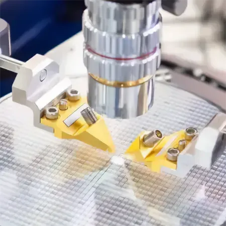
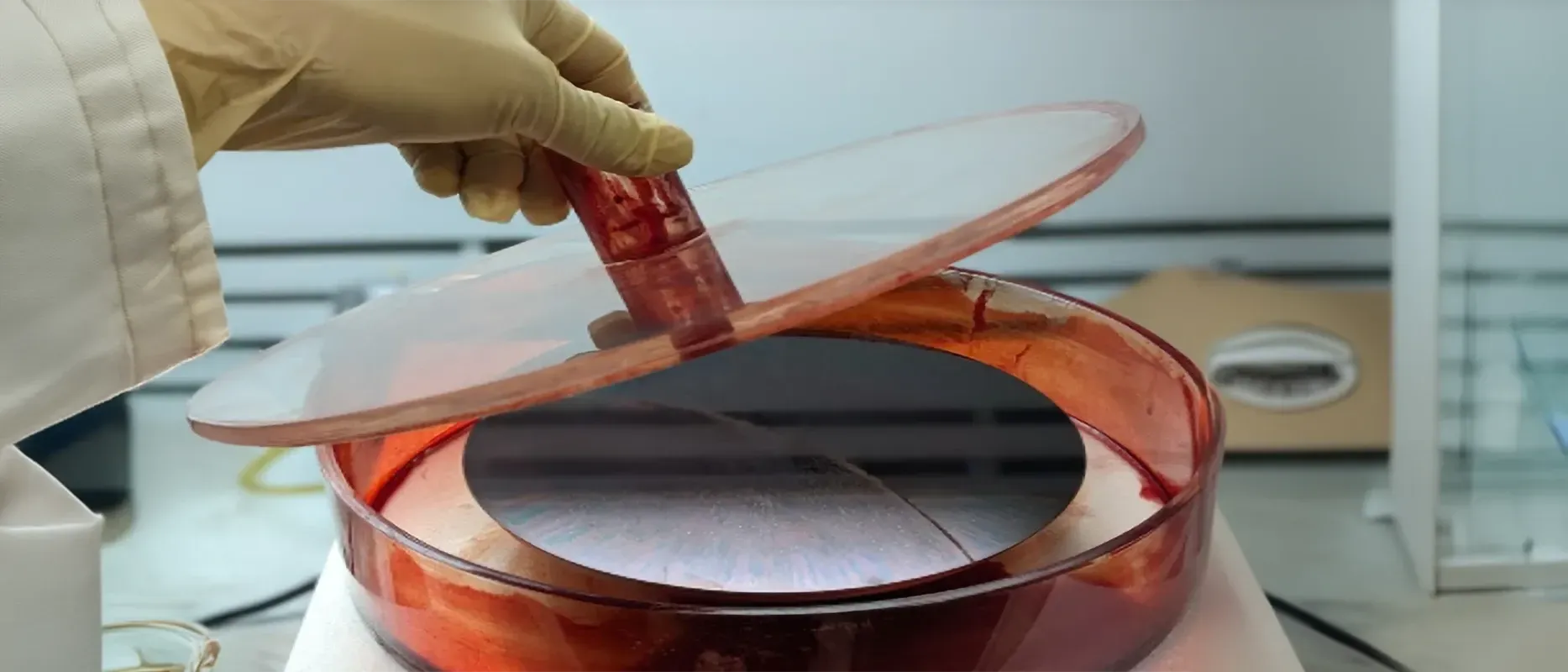
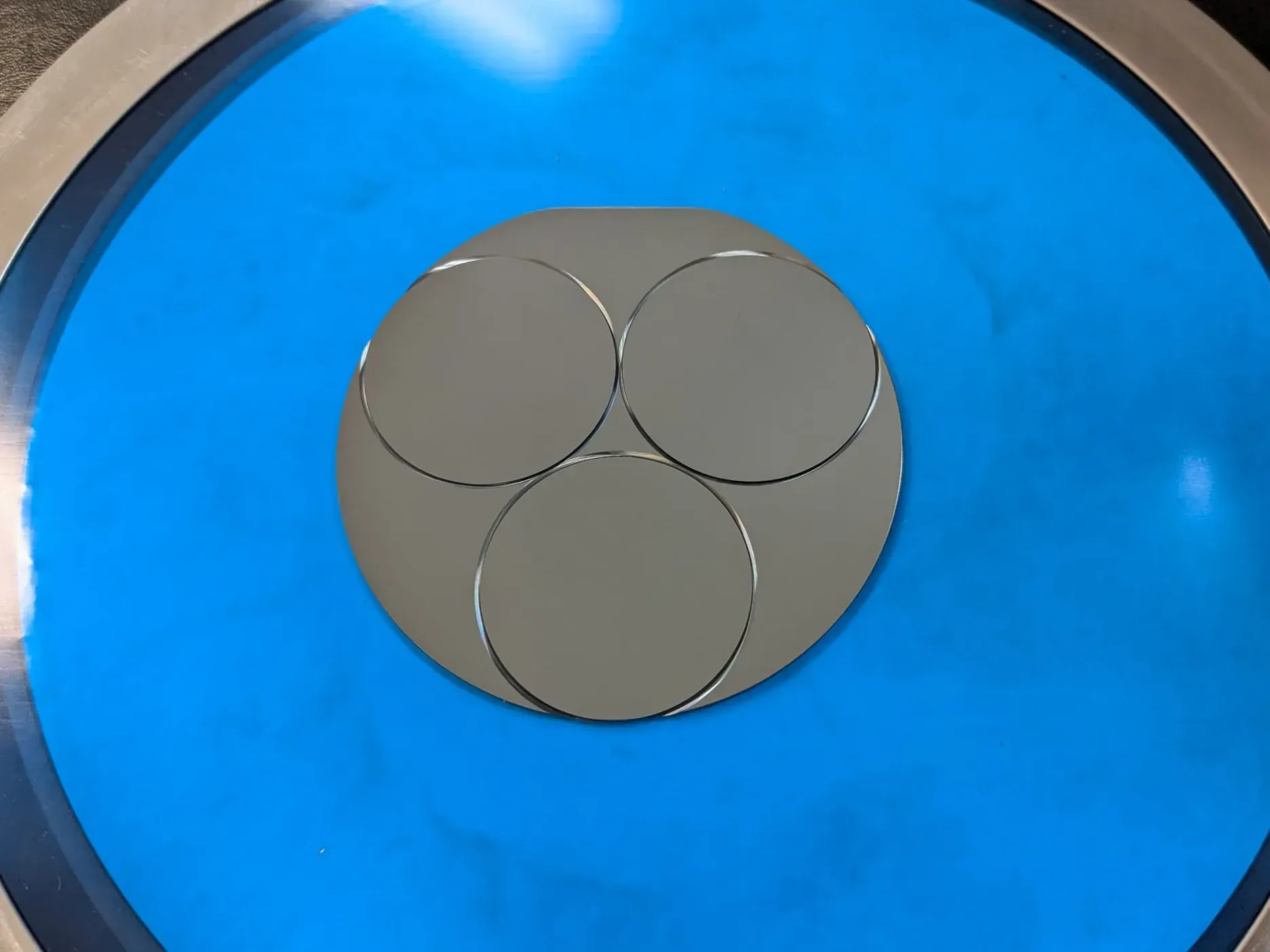
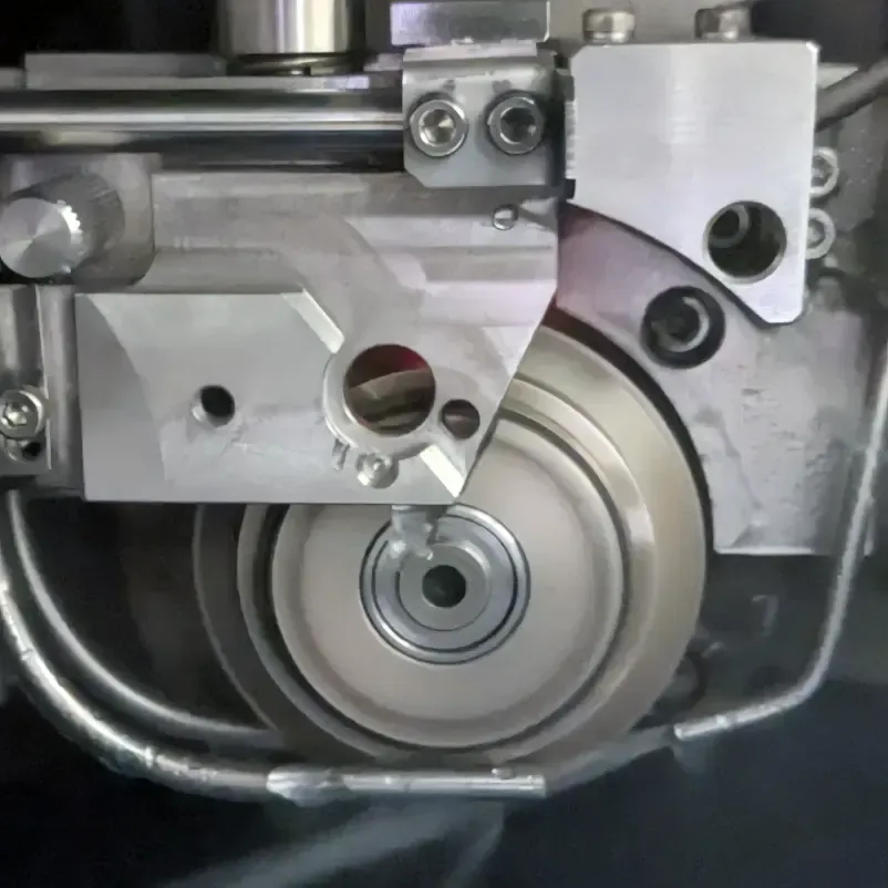
Depaneling Using Wafer Dicing Saws
Wafer dicing saws are precision tools that cut PCBs along predefined lines, offering excellent accuracy and control. This method is ideal for straight cuts but is limited when dealing with curvilinear or intricate designs, which is where laser depaneling would be a better fit. Wafer dicing is particularly effective for projects requiring high precision, especially when working with fragile materials or where clean, smooth edges are essential.
The Importance of Depaneling
Depanelization is a crucial step in PCB manufacturing, facilitating the efficient production of large numbers of PCBs while maintaining quality. Choosing the right depaneling method based on the project’s specific requirements can significantly impact both the cost and the final product's integrity.
How to Choose the Right Depaneling Method
Selecting the appropriate depaneling method depends on several factors, including:
1. The size and complexity of the PCBs
2. The volume of PCBs to be processed
3. Cost considerations
4. Required accuracy and precision
By weighing these factors, manufacturers can select the most suitable depaneling method to meet their specific needs.
Why Choose APD for PCB Depaneling?
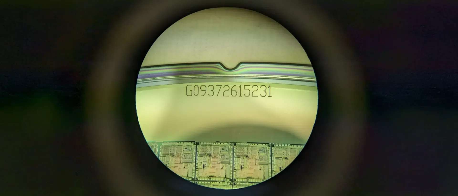
At American Precision Dicing, we are experts in the depaneling of printed circuit boards. Our dicing saw process guarantees an impressive accuracy of +/- 10 microns, ensuring clean, flawless cuts, even for intricate designs. With the capability to create kerfs smaller than 200 microns, depending on the PCB thickness, our precision technology maximizes material utilization and supports complex designs.
Moreover, our comprehensive services extend beyond cutting. We ensure that the depaneled boards are meticulously picked, placed in custom containers, and prepared for further assembly or shipment. Understanding the industry's fast-paced nature, we prioritize quick turnarounds without compromising quality.
Conclusion
Depanelization is a key component in PCB manufacturing, and choosing the right method can greatly influence the final product's quality and cost. At APD, we provide precise and efficient depaneling services tailored to meet your specific requirements. Whether your project demands high-volume production, intricate designs, or fast turnarounds, our team has the expertise and technology to deliver exceptional results.
Interested in learning more about our PCB depaneling services?
Contact us at +1(408)539-9880, sales@wafer-dicing.com, or visit our Request a Quote page to get in touch with our team. We're here to provide the precision and quality your project demands!