Precision and Expertise in Wafer Dicing Services at APD
Expert Wafer Dicing Services for Semiconductor Manufacturing
Proven Excellence in Wafer Dicing
In the intricate world of semiconductor manufacturing, precision and reliability are paramount. At American Precision Dicing, Inc. (APD), we have honed the craft of wafer dicing since 1999, delivering unparalleled service to a diverse clientele. Our commitment to excellence has established us as a leader in the industry, catering to universities, research labs, and major corporations. This blog post delves into our wafer dicing service, highlighting our meticulous process and the unique advantages we offer.
The Process of Wafer Dicing
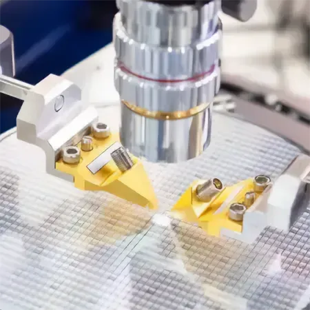
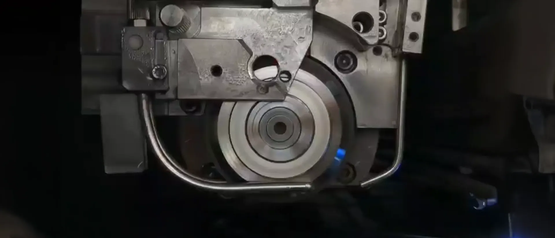
Wafer dicing involves the separation of individual semiconductor dies from a larger wafer, a critical step in semiconductor manufacturing. At APD, we utilize precision mechanical dicing saws equipped with diamond blades to achieve this with exceptional accuracy. Our process is designed to handle various hard and brittle materials, including silicon, glass, ceramics, sapphire, and silicon carbide.
Our Comprehensive Dicing Process
1. Material Preparation
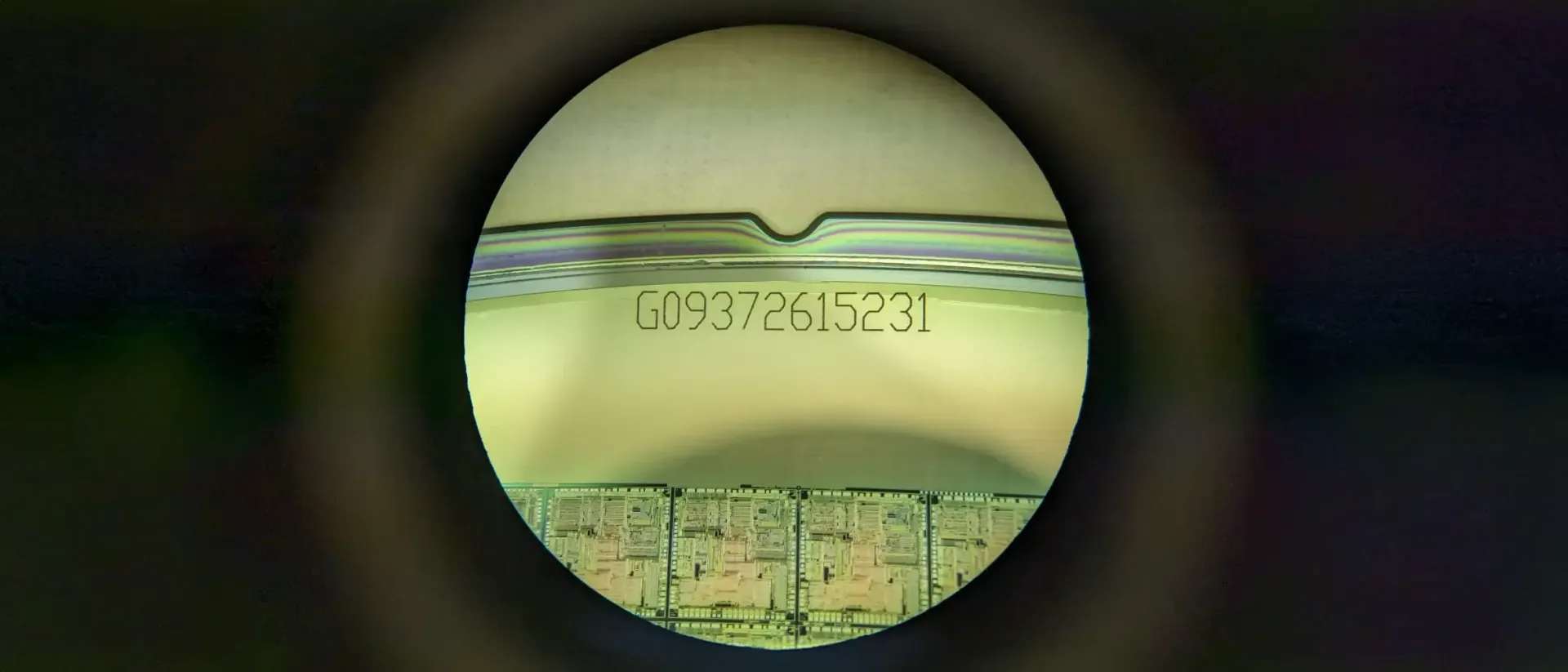
Our process begins with thorough material inspection and preparation. Each wafer is carefully examined to identify any defects or irregularities that might affect the dicing process.
2.
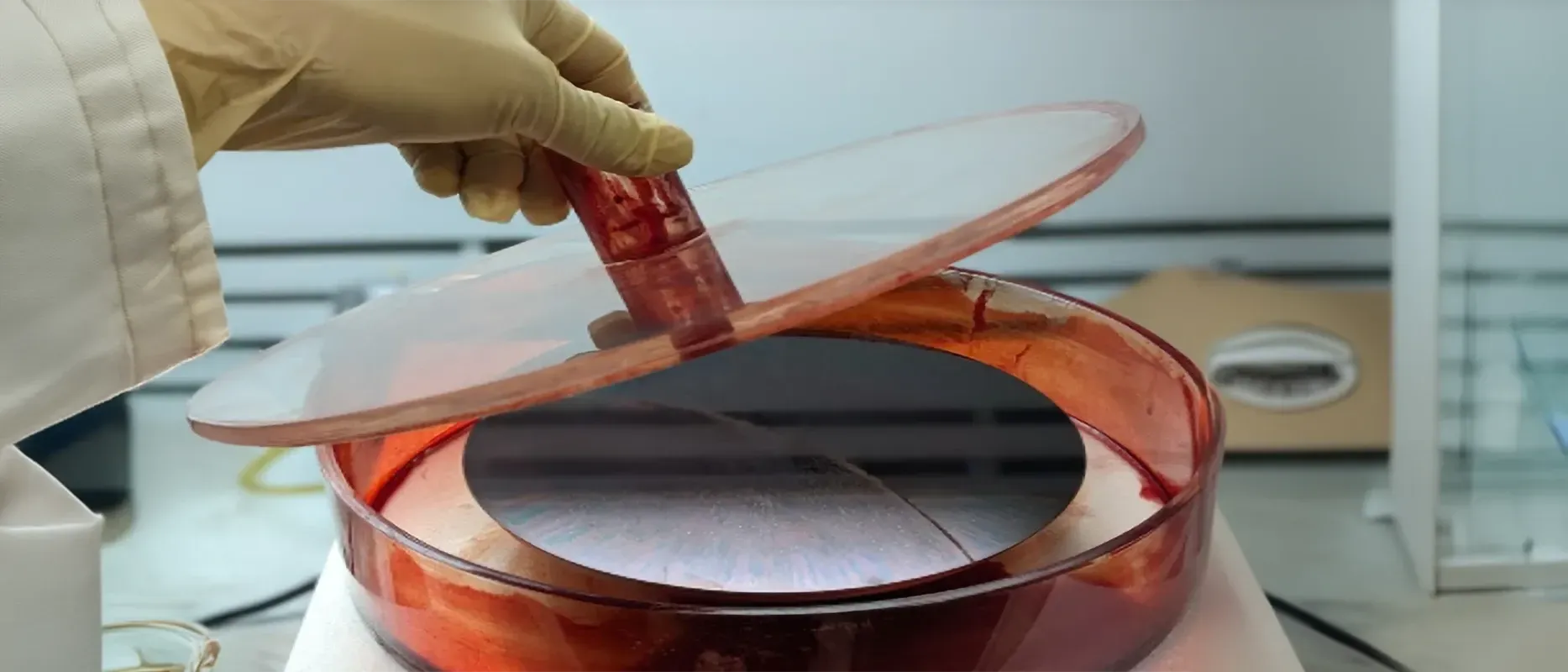
Surface Protection
In cases where the wafer surface needs protection from downstream processes, we apply a layer of photoresist. This step ensures the integrity of the wafer throughout the dicing process.
3.
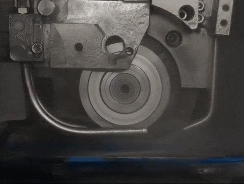
Precision Dicing
Using our state-of-the-art mechanical dicing saws, we perform the dicing with remarkable precision. The diamond blades cut through the wafer with minimal kerf loss, ensuring that each die is separated cleanly and accurately.
4.
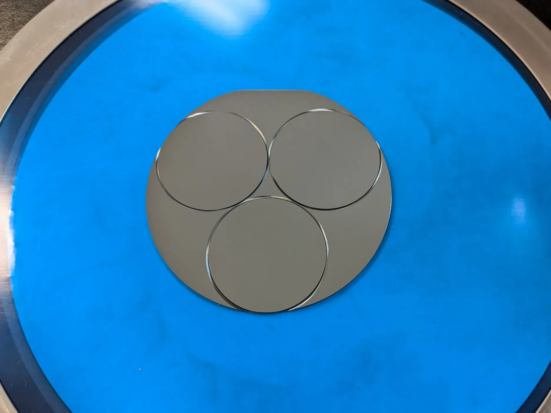
Die Sort, Pick, and Place
Post-dicing, our die sort, pick, and place service comes into play. This process involves the careful selection and placement of individual dies, ensuring they are ready for further processing or assembly. Our meticulous sorting and labeling enhance the efficiency of the entire manufacturing process.
5.
Quality Assurance and Packaging
Every diced wafer undergoes rigorous quality assurance checks to ensure it meets our high standards. We then package the dies securely, ready for shipment to our customers.
Advanced Capabilities and Custom Solutions
At APD, we pride ourselves on our ability to handle both standard and custom wafer dicing projects. Our advanced equipment and expertise allow us to offer tailored solutions that meet the specific needs of our clients. Whether it’s resizing a wafer or achieving unique geometries, we are equipped to deliver exceptional results.
Service Principles: Speed, Value, and Flexibility
Our service principles of speed, value, and flexibility drive our operations. We offer same-day service for urgent wafer dicing needs and next-day shipping with overnight delivery. Our experienced team and advanced machinery ensure maximum efficiency and accuracy, while our commitment to customer satisfaction guarantees competitive pricing and customized solutions.
Why Choose APD?
Choosing APD means partnering with a company that prioritizes precision, reliability, and customer service. With decades of experience and a proven track record, we are dedicated to exceeding expectations and delivering top-tier wafer dicing services.
Get Started Today
Ready to experience the APD difference?
Contact us today to discuss your wafer dicing needs or
request a personalized quote through our website. Let us help you achieve unparalleled precision in your semiconductor manufacturing process.