The Importance of Wafer Coring in Semiconductor Manufacturing
The Wafer Coring Process at APD
In the semiconductor industry, adapting to evolving technologies and equipment is crucial. At American Precision Dicing, Inc. (APD), we specialize in wafer coring, a process essential for resizing wafers to fit specific processing equipment. This blog post delves into the intricacies of wafer coring, its significance, and why APD is your trusted partner for this critical service.
What is Wafer Coring?
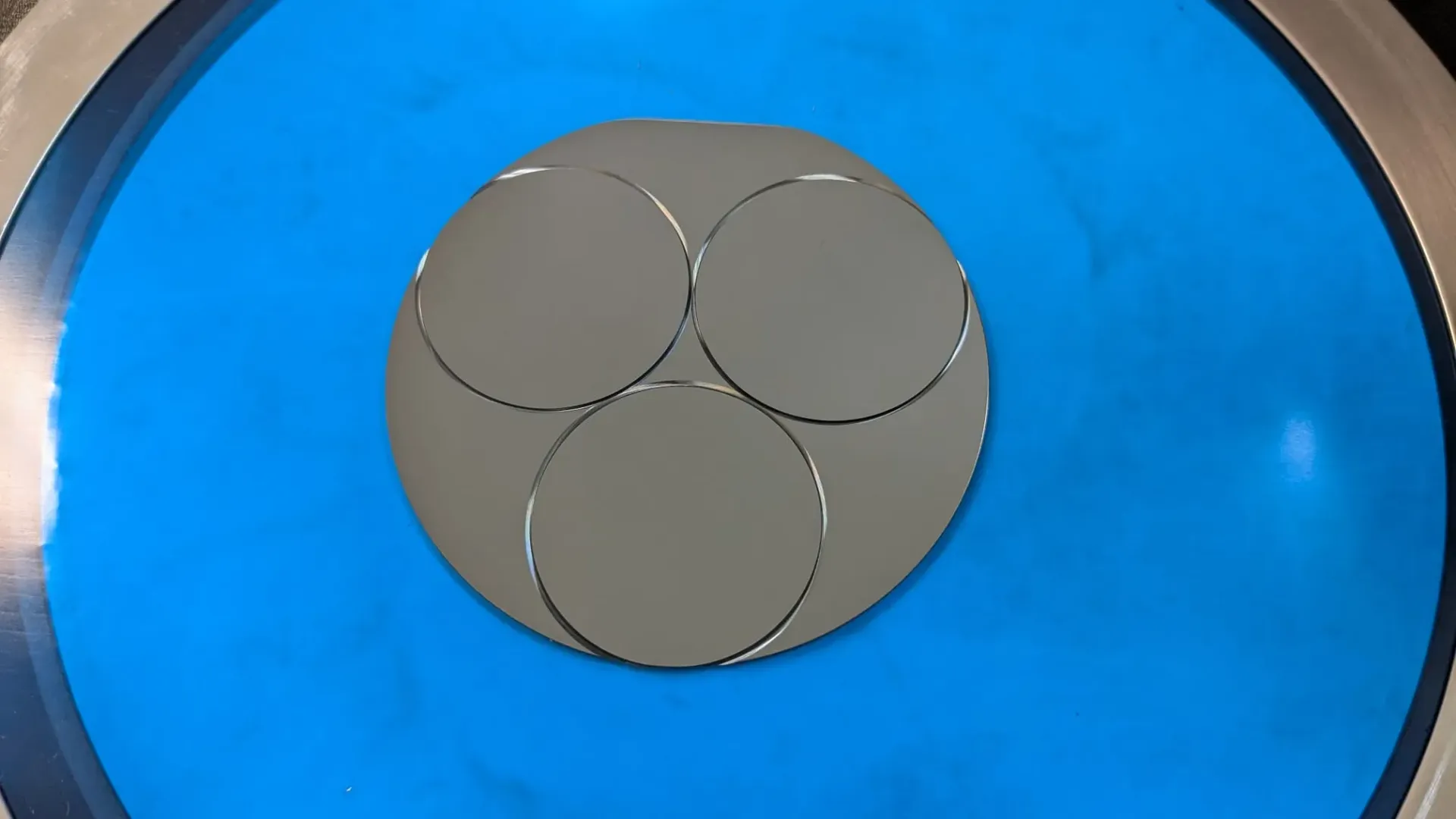
Wafer coring, also known as wafer resizing, involves reducing the diameter of a wafer to fit the available processing equipment. This process ensures that older, expensive tooling remains usable despite changes in wafer sizes.
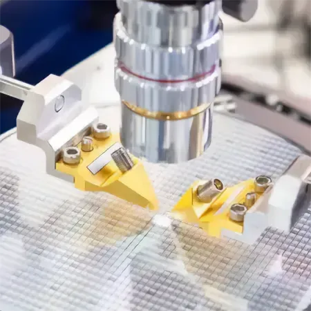
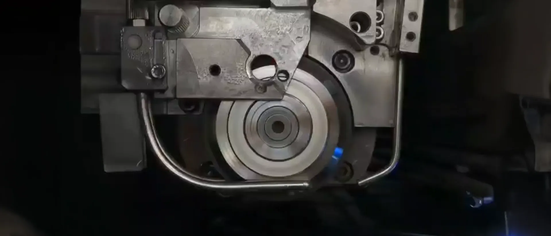
The Wafer Coring Process
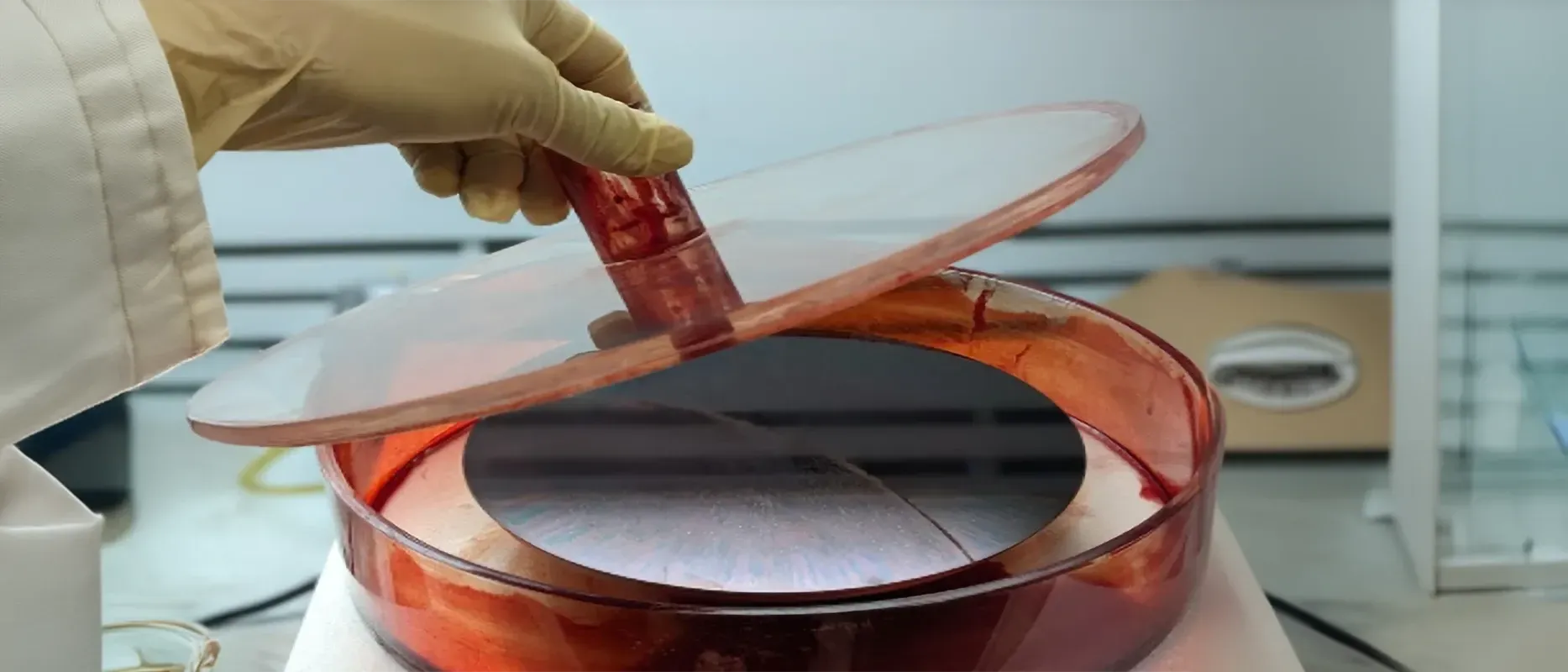
- Preparation: A protective layer is applied to the wafer to prevent surface damage.
- Grinding: Wafers are ground to the required thickness if necessary.
- Custom Programming: A custom coring program is created based on specific customer requirements.
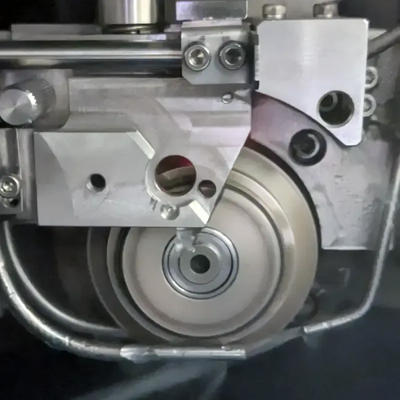
- Coring: The wafers are resized using mechanical sawing processes.
- Edge Beveling: Resized wafers are edge-rounded to enhance mechanical stability.
- Inspection: Detailed inspections ensure quality and precision.
- Cleaning and Packaging: The protective layer is removed, and the wafers undergo a thorough cleaning before packaging and shipment.
Why Choose Mechanical Coring Over Laser?
Mechanical coring offers flexibility in handling various hard and brittle materials such as silicon, glass, and sapphire. Unlike lasers, mechanical cutting does not require adjustments based on the material's properties, making it more versatile and cost-effective.
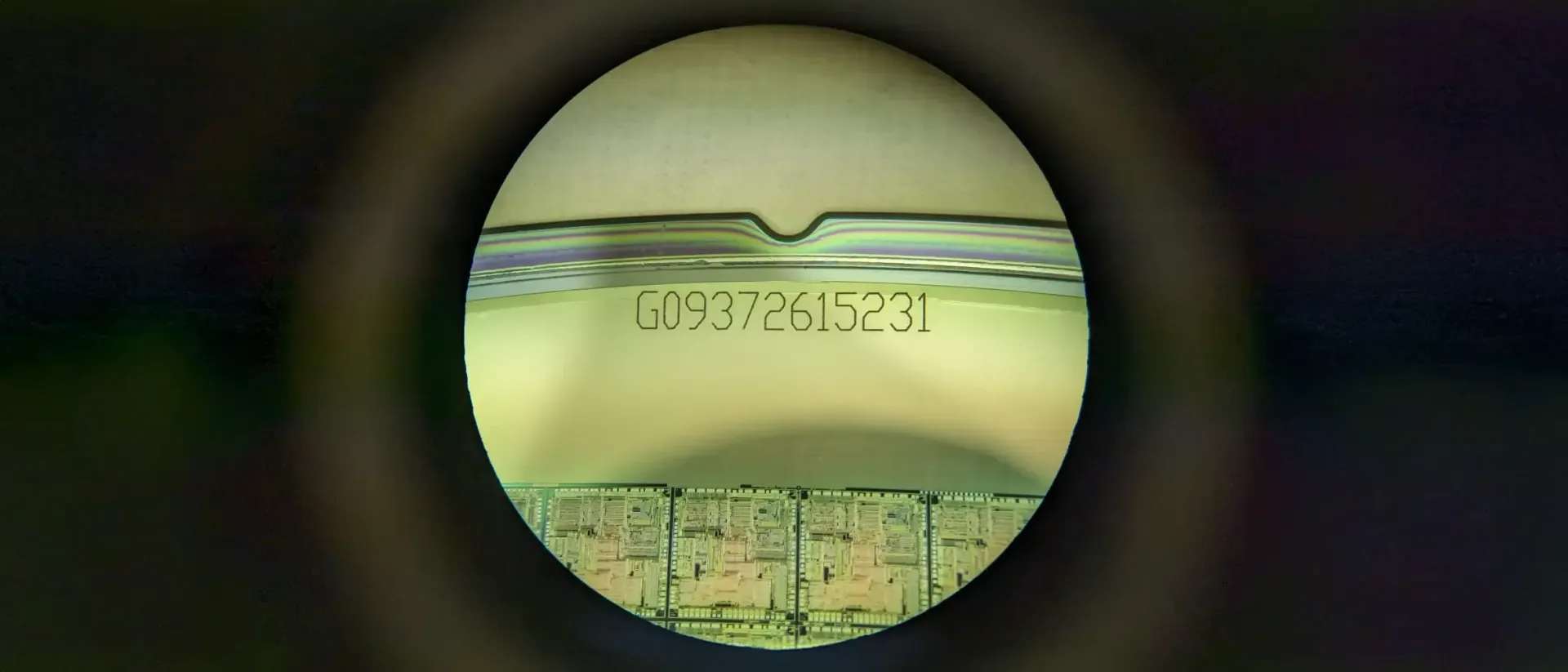
Flats and Notches
Wafer flats and notches are critical for alignment and indicate the wafer's crystal orientation. Maintaining these features during coring is essential for the integrity of the wafer's function and alignment in subsequent processes.
Advanced Capabilities
At APD, we handle wafers up to 300mm in diameter, resizing them to standard sizes such as 2", 3", 4", 6", 8", and 12". Our expertise extends to various materials, ensuring precise and reliable resizing for both patterned and blank wafers.
Why APD?
Choosing APD means partnering with a company that values precision, reliability, and customer satisfaction. Our comprehensive wafer coring services, advanced capabilities, and dedication to excellence make us the ideal choice for your semiconductor manufacturing needs.
Conclusion
Wafer coring is a critical component in semiconductor manufacturing, enabling the continued use of existing processing equipment despite changes in wafer sizes. At APD, we excel in providing high-quality, precise wafer coring services tailored to your specific requirements. Contact us today to learn more about our wafer coring services and how we can support your manufacturing processes.
For more detailed information, visit our
Wafer Coring Service Page.