Precision Dicing for 300mm (12-inch) Wafers
Precision Dicing for 300mm Wafers: Enhancing Semiconductor Efficiency
In the semiconductor industry, the transition from 200mm to 300mm wafers has revolutionized production efficiency. At APD, we specialize in the precision dicing of 300mm wafers, which allows manufacturers to significantly increase yield and reduce costs.
Understanding Wafer Dicing and Slicing
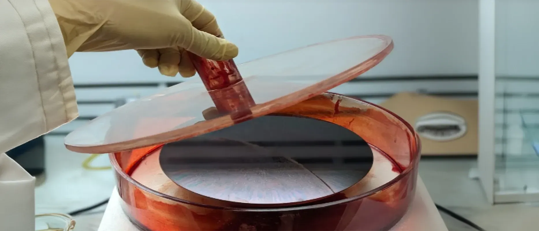
Wafer Slicing: This initial step involves slicing a silicon ingot into thin wafers, typically using diamond-studded wires or large blades. The sliced wafers then undergo a series of processes to become ready for dicing.
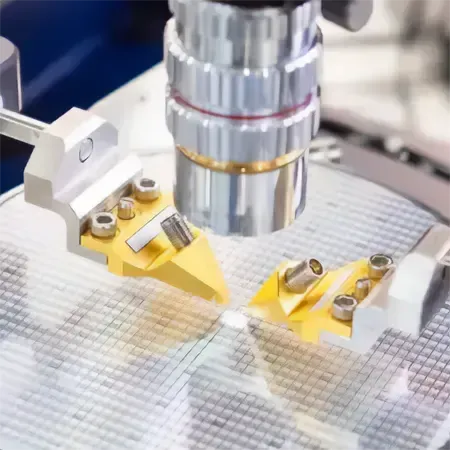
Wafer Dicing: This final stage in semiconductor fabrication involves cutting the wafer into individual dies or chips. APD utilizes advanced mechanical sawing techniques with diamond blades to achieve high precision, although other methods like laser dicing are also available depending on the material and requirements.
The Significance of 300mm Wafers
Why 300mm? The primary advantage of using 300mm wafers over 200mm wafers is economic efficiency. A larger wafer size allows for more dies to be cut from a single wafer. For instance, a 200mm wafer yields about 240 dies (assuming each die is 1 cm²), while a 300mm wafer yields over 570 dies, more than doubling the yield with just a 50% increase in wafer diameter.
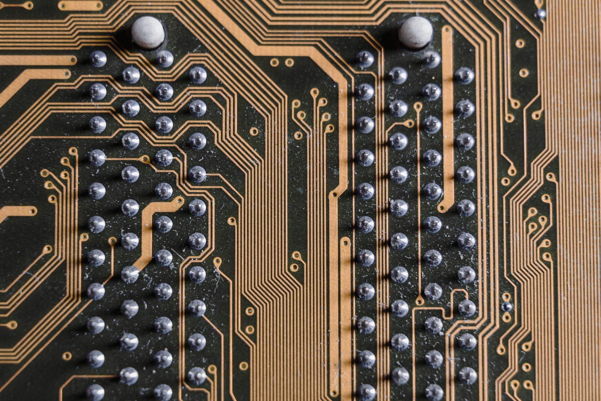
Material Flexibility: While silicon is the most common material used, APD also handles other hard, brittle materials such as silicon carbide, glass, and sapphire. These materials offer unique properties, such as enhanced thermal management or transparency for optical devices.
APD's 300mm Wafer Dicing Services
APD offers a comprehensive suite of services for 300mm wafer dicing, including:
Mounting:
Securing the wafer for the dicing process.
Dicing:
Cutting the wafer into individual dies with precision.
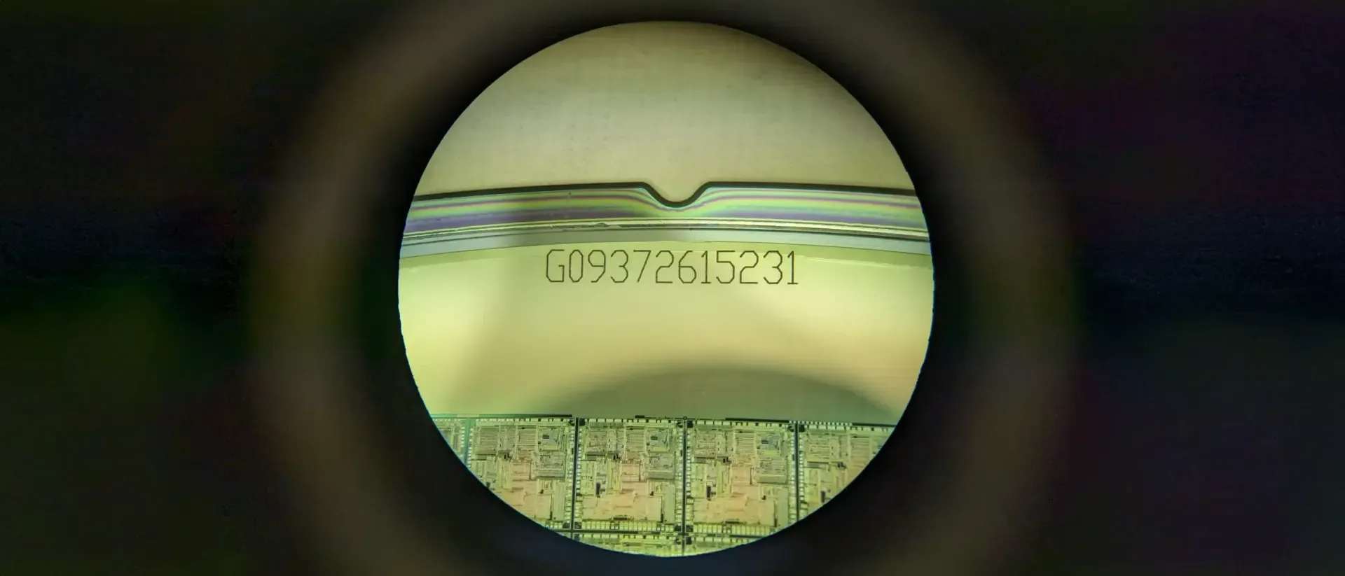
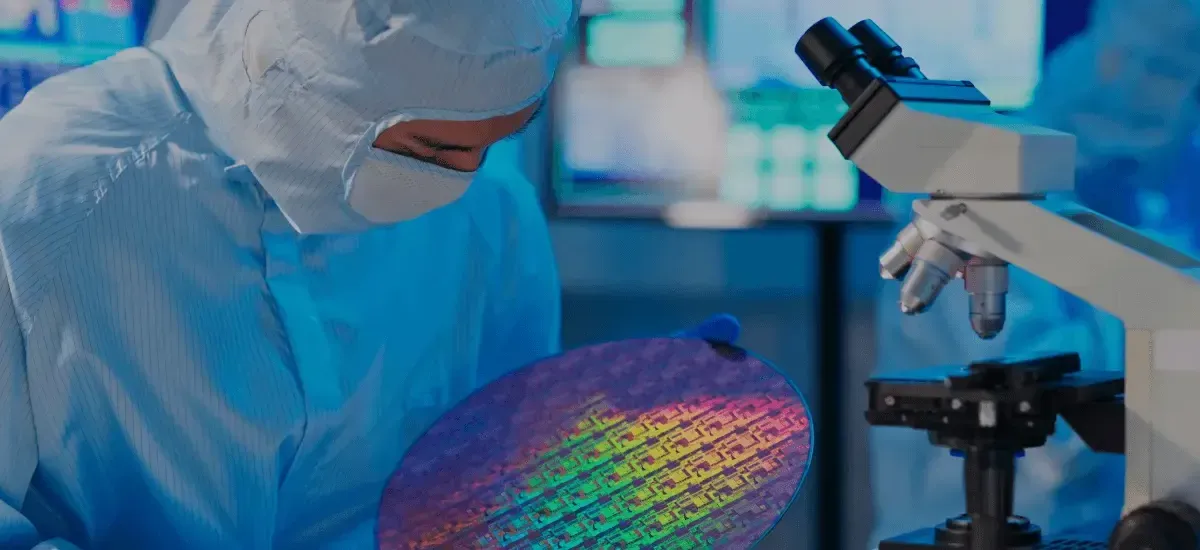
Inspection: Ensuring each die meets stringent quality standards.
Sorting and Picking: Organizing the known good dies for further processing.
Placing: Carefully positioning dies into various types of trays like waffle packs or gel packs.
Packaging: Preparing the dies for safe transport and further use.
In addition to dicing, we also manage outside services like
backgrinding and
photoresist application, ensuring a seamless experience for our clients.
Why Choose APD?
1.
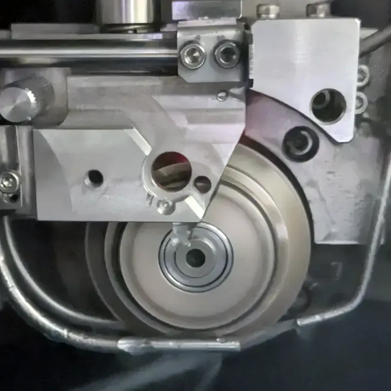
Cutting-Edge Technology: Our state-of-the-art dicing equipment offers absolute accuracy within ±2 microns and repeatability within ±1 micron. The spindle speed reaches up to 60,000 RPM, nearly double that of older machines, ensuring faster and cleaner cuts.
2.
Advanced Features: Our systems use artificial intelligence to monitor and optimize the kerf check function, ensuring consistent quality. With the capability to store up to 10,000 process parameter combinations, we offer unmatched flexibility and reliability.
3.
Rapid Turnaround: We understand the pressures of tight deadlines. Our efficient processes and advanced technology enable us to deliver exceptional results with minimal lead times.
If you're interested in 300mm or 12 inch wafer dicing, contact us at +1(408)539-9880, sales@wafer-dicing.com, or visit our Request a Quote page to get started. Let us take care of the details, so you can focus on what you do best.